Our ALU is required to support four integer arithmetic operations: Signed Addition (ADD), Unsigned Addition(ADDU), Signed Subtraction (SUB), and Unsigned Subtraction (SUBU). For signed operations, the inputs and output will be treated as 32-bit signed twos-complement integers.
| Operation | ALUOp(1) | ALUOp(0) |
|---|---|---|
| ADD | 0 | 0 |
| ADDU | 0 | 1 |
| SUB | 1 | 0 |
| SUBU | 1 | 1 |
We can make use of several properties of signed twos-complement
numbers to significantly reduce the hardware requirements of
our Aritmetic sub-block without significantly decreasing
its speed. In fact, we can implement all four of the
necessary operations using a single 32-bit adder!
Let's start by examining the signed vs. unsigned issue.
The hardware
for adding or subtracting twos-complement signed integers
and magnitude representation unsigned integers is actually
exactly the same. The only difference comes in determining
when Overflow occurs. Overflow is
the condition where the result of the operations is either
too large or too small to be represented in the alotted
number of bits (32). For signed numbers, overflow can
only occur when adding two numbers of the same sign or
subtracting two numbers of opposite signs. It is indicated
for addition by the result having the opposite sign of
the inputs and in subtraction by the result having the
opposite sign of the first input. In unsigned numbers,
and overflow would be indicated by a carry-out from the
most significant bit.
A trickier issue is how we can perform both addition and
subtraction with just a single 32-bit adder. The answer
comes by restating the operation: A - B = A + (-B).
We can negate a twos-complement number by inverting the
bits and adding one: (-B) = NOT(B) + 1. So,
A - B = A + (-B) = A + NOT(B) + 1. By adding
and inverter and a multiplexor (to select B or NOT(B))
in front of the B input we can implement A + B
or A + NOT(B) easily. To add one, we take
advantage of the fact that our adder has a carry-in.
By carrying in a '1', we are effectively adding one
to the result. This
trick also works out for unsigned subtraction.
To create the Arithmetic sub-block we will need to have a 32-bit adder with carry-in, carry-out, and overflow computation. Instead of going through the process of building this from scratch, we will be using an adder which has already been designed and instantiating it as a Component in our design.
You have already seen that the blue colored sub-blocks which
you have placed in the ALU block diagram generate entity
declarations with corresponding architectures created from
their views which are then instantiated in the ALU
architecture as components. In FPGA Advantage, however,
these sub-blocks are not referred to as components because
you cannot instantiate them in another design as they are;
they are tied to one instance in one design. A sub-block
can, however, be converted into a FPGA Advantage component,
represented by a green colored box. They are essentially
the same except for the fact that a component can be accessed
from other design units to be instantiated.
Components allow for the creation of design libraries of
commonly used objects which can be instantiated in new designs.
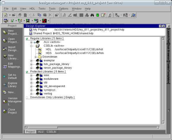
I have created a 32-bit adder component and placed it in the
CSELib library, which holds public design components that we
will be using.
It is not necessary for a library to be open in the Design
Manager in order to instantiate a component from it.
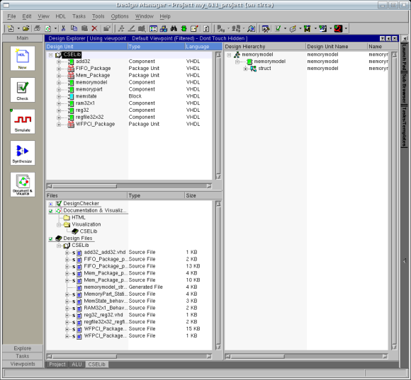
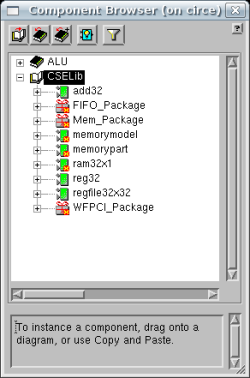
In order to see what is in the library, though, click on
the Project tab on the bottom of the Design
Manager. Within that window, double-click on the
CSELib under Protected Libraries. Design Explorer
will now open up the CSELib so that you may
browse it. Expand the design tree in the source window
to see a single design unit, in green, called add32
with a symbol, an VHDL Entity and VHDL Architecture
view called add32. The Design Manager window
will look like the figure below:
Now that we know what's in the CSELib library,
we can get started designing the Arithmetic unit.
Go back to your ALU design by clicking on the tab
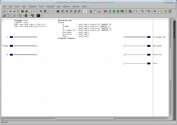
below and opening the design. Once you have done this,
create a new block diagram view for the Arithmetic
sub-block by double-clicking on the sub-block and
selecting Block Diagram from the window that opens.
Click Next and then Finish. This will bring
up the block diagram with ports seen in the figure below:
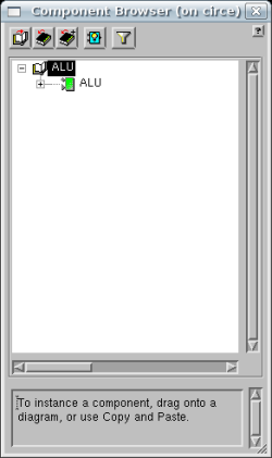
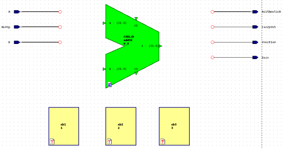
Now we wish to instantiate an add32 component. Activate the
Add Component tool by selecting the button,
 , from the toolbar.
This will bring up the Component Browser window which
will allow you to select which component to instantiate.
, from the toolbar.
This will bring up the Component Browser window which
will allow you to select which component to instantiate.
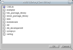
Click the Add Library button,  ,
then select the CSELib library and click OK.
,
then select the CSELib library and click OK.
You will then see a list of the components in this library.
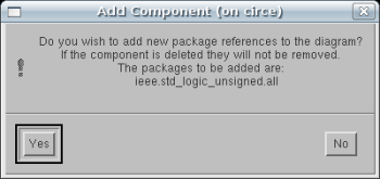
Drag and drop the add32 component into your design.
You will now see a message box pop up asking whether
you wish to add packages to your design. This is a VHDL package
which is used in the adder. Respond yes to move on.
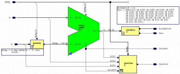
In addition to the ADD32 component, there are several
other tasks which need to be accomplished: selecting B
or NOT(B) and deciding whether to carry-in a '1' to
configure for addition or subtraction; deciding whether or
not to compute overflow; and calculating Zero which is
high whenever the result is equal to zero and low otherwise.
These tasks will be implemented using Embedded Blocks
just like in the Logical sub-block. We need to place
After adding these blocks your block diagram should look like
the figure below:
Now that the embedded blocks and the add32 component
have been placed on the block diagram, connect the input and
output ports and create the necessary internal signals so that
the block diagram resembles the figure below:
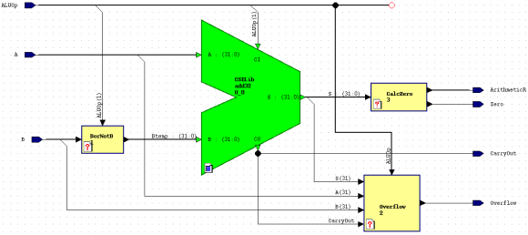
The final step, after all signals are connected properly
is to define the behavior of the embedded blocks. Two of the
three blocks will have a behavior of text where as the Overflow
block will encorporate a truth table. Double-click on the
embedded blocks and set their associated behavior. The embedded
block behaviors are as follows:
    Btemp <= B when ALUOp(1) = '0' else
             not(B);
This embedded block implements a multiplexor with B as
the input when the select, ALUOp(1), equals zero to implement
an add and NOT(B) when the select equals one to
implement a subtract. The other step necessary to implementing
subtraction, carrying in a one, is taken care of by
connecting ALUOp(1) to the carry-in of the adder. This
way, when adding the carry-in is zero and when subtracting
the carry-in is one.
    ArithmeticR <= S;
    Zero <= NOT(S(31) OR S(30) OR S(29) OR S(28) OR S(27) OR S(26) OR S(25)
    OR S(24) OR S(23) OR S(22) OR S(21) OR S(20) OR S(19) OR S(18) OR S(17)
    OR S(16) OR S(15) OR S(14) OR S(13) OR S(12) OR S(11) OR S(10) OR S(9)
    OR S(8) OR S(7) OR S(6) OR S(5) OR S(4) OR S(3) OR S(2) OR S(1)OR S(0));
This block contains two VHDL statements, necessary
because we cannot simultaneously assign the
output of the adder directlyto ArithmeticR
and at the same time use that value to determine
the Zero output. The first statement
takes the internal value of the adder output,
S, and assigns it to the result,
ArithmeticR. The second statement
determines whether the adder output is equal to
zero by ORing the individual bits together.
If the result of the OR is '0', meaning the
result is zero, we want to output a
'1' and if the result of the OR is a '1',
meaning the result is non-zero, we want to
output a '0'. Thus we invert the result of
the OR to obtain our Zero output.
Your arithmetic sub-block should now resemble the figure below:
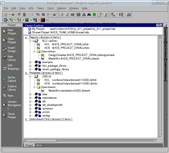
Before we attempt to compile and simulate the Arithmetic Sub-Block we must make a change to FPGA Advantage. Currently the downstream, or temporary working directory that FPGA Advantage and ModelSim use to place compiled files, is set to the default directory in the CSElib library mapping /usr/local/3rdparty/csce611CSElib/work. However, since students do not have write access to this directory FPGA Advantage will not be able to compile the add32 component. To change the downstream mapping, go to the Design Manager window and select the Project tab the bottom. Your window will look something similar to the figure below:
You may have to select the plus symbol next to CSElib to expand the
tree of library mappings and then select the plus symbol next to
Downstream to show the current Downstream mapping for ModelSim.
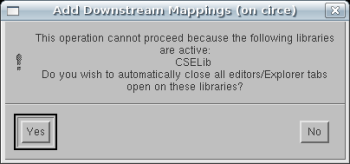
Right-click on Downstream and select "Add Downstream mapping...". You
may see the following window. If so, click "Yes".
You will then see the following window. Select "Modelsim", then use the
path as shown, but substitute "username" with yours:
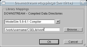
Note: Unfortunately, this directory needs to be
manually created in order for any components in the
Protected Library to be compiled. Please remember
to recreate this directory if you continue your
work on a different PC. Here is a simple command
to create your required downstream mapping:
mkdir -p /work/username/CSELib/work
Don't forget to change "username" to yours.
Your Design Manager should now look like this:
Now that we have designed the Arithmetic sub-block, we
must of course verify that it is functioning correctly. Since
we are once again dealing with a fairly small design unit, we
will test it by directly stimulating the signals in the simulator
and observing the results in the Waves window.
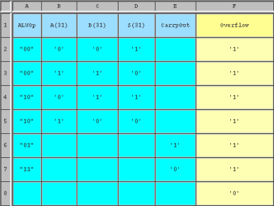
You will need to create a simulation macro file (do file) which will
run at least one set of vectors to test each possible outcome of
each operation:
You may find it helpful when trying to create your test vectors
to use a calculator. Most calculator programs allows you to convert
between decimal and signed twos-complement binary representations of
numbers.
Create and run your test macro to confirm the function of your
Arithmetic unit. Comment your macro file to indicate
the decimal equivalents of the test vectors as well as
the expected values of ArithmeticR, Zero, and
Overflow.
When you have finished, you are ready to go on to..