[print this page]
Adding Subblocks to the Block Diagram
Before we can add any logic or structure to our ALU, it would be wise to
stop and formulate an overall plan for how we will have the ALU accomplish what
it needs to do.
First of all, let's examine the functions which the ALU is expected to
perform. There are 13 different functions, each of which requires its own
unique ALUOp code. Since a 3-bit ALUOp could only supply encodings for 8
operations, we are required to use a 4-bit ALUOp code which allows for encoding
16 possible operations, hence there will be 3 codes which will not be used.
Furthermore, the functions can be conveniently grouped into four categories:
| LOGICAL |
(AND, OR, NOR, XOR) |
| ARITHMETIC |
(ADD, ADDU, SUB, SUBU) |
| COMPARISON |
(SLT, SLTU) |
| SHIFT
| (SLL, SRL, SRA) |
In order to increase the speed at which our ALU operates, many different
computations will be performed simultaneously and the desired result will be
selected by a multiplexor at the output end of the ALU. Since we have four
operation types, each of which contains no more than four distint operations, a
natural hierarchy presents itself. Our first design decision will be to create
four blocks on the top level diagram, each of which will produce the proper
output for one of the operation types. We will place a fifth block which will
multiplex these four intermediate results into a final output of the ALU. We
will assign the upper two bits of the ALUOp, ALUOp(3 downto 2), as the select
lines of this output multiplexor which determines which class of operation is
performed. The output of this 32-bit wide 4-1 mux will be the result, R. The
encodings for ALUOp(3 DOWNTO 2) to function classes are found in this table:
| ALUOp3 |
ALUOp2 |
Function Class |
| 0 |
0 |
Logic |
| 0 |
1 |
Arithmetic |
| 1 |
0 |
Comparison |
| 1 |
1 |
Shift |
Within each operation class block, the exact operation which is output as
the intermediate result is determined by the lower two bits of the ALUOp,
ALUOp(1 downto 0). We will examine the encodings of these two bits for each
operation class as we create the logic for that block.
Adding the Subblocks
It is clear then that the top level block diagram will require 5 subblocks:
Logical, Arithmetic, Comparison, Shifter, and
Mux4Bus64.
To place a subblock on the block diagram, first highlight the Add Block,
 , button from the
toolbar. Now, move the pointer over the design area to a point somewhat to the
right of the input ports and signals which you have already placed on the
diagram and left-click to place a block. This block will appear as a blue
rectangle with identifying text inside: the library name ALU; a default
block name and a default instance label U_0. Deselect the Add
Block tool and open the Object Properties window by right-clicking
over the block and then selecting Object Properties from the pop-up
menu. Under the name field, enter Logical, you may leave the Instance
name unchanged. When you have made this change, click OK.
, button from the
toolbar. Now, move the pointer over the design area to a point somewhat to the
right of the input ports and signals which you have already placed on the
diagram and left-click to place a block. This block will appear as a blue
rectangle with identifying text inside: the library name ALU; a default
block name and a default instance label U_0. Deselect the Add
Block tool and open the Object Properties window by right-clicking
over the block and then selecting Object Properties from the pop-up
menu. Under the name field, enter Logical, you may leave the Instance
name unchanged. When you have made this change, click OK.
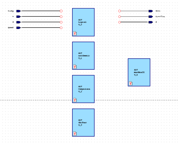
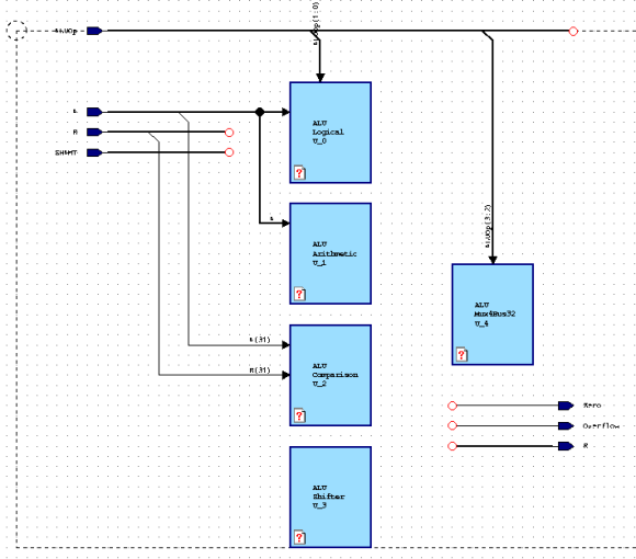
Now place four more blocks onto the diagram: three in a column
below the Logical block and one more to the right of this column
and centered vertically between the second and third blocks. Label
the column blocks, from top to bottom below Logical: Arithmetic,
Comparison, and Shifter. Then label the lone block on the
right Mux4Bus32. Your block diagram should now resemble the
figure below:
To complete the top level block diagram, we need to wire the input and output
port signals to the blocks which we just defined and also wire the blocks
together using some purely internal signals and busses.
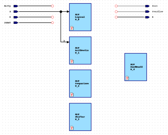
First, select the Add Bus tool. Move the pointer over the open circle
at the dangling end of the A bus and left-click. Now move the pointer to
the left edge of the Logical block and left-click again to connect this
bus to the block. Next move the pointer to any place along the A bus and
left-click. Then move to the left edge of the Arithmetic block and left
click to create a spur off of that bus connecting it to the second block. A
is now connected as an input to both the Logical and Arithmetic
blocks and your diagram should resemble the figure below:
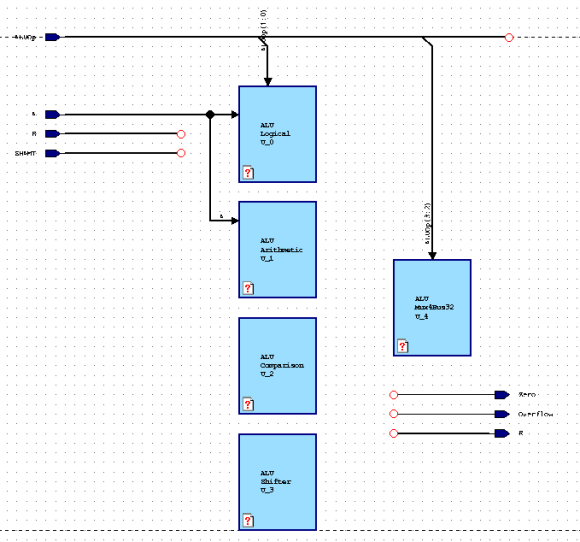
With the select tool active, move the ALUOp bus so that it is above all of
the blocks on the diagram. Select the dangling end of the bus and drag it
to the right to extend the bus almost the full length of the block diagram.
We do not actually want all four bits of the ALUOp bus to be connected to
the Logical block, since only bits zero and one are used to
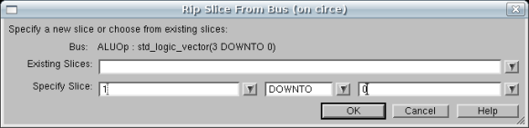
control it. In order to limit which signals are connected, we will define the
segment which extends down to the block as a slice of the ALUOp bus. To
do this, click the down-arrow on the bus button  and select the slice button
  . Use it to
draw a bus down from the ALUBus and connect it to the Logical Block. Specify
the slice as 1 downto 0.
. Use it to
draw a bus down from the ALUBus and connect it to the Logical Block. Specify
the slice as 1 downto 0.
Repeat this process to connect ALUOp(3 DOWNTO 2) to the Mux4Bus32 block.
Your block diagram should now resemble the figure below:
For reasons to be explained later, the Comparison block will only
require the highest order bits from the A and B busses. Activate
the Add Signal tool and Left-click over a spot on the A bus to
pull a single signal off of the bus. Connect this signal to the left side of
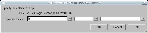
the Comparison block. Once you click on the Comparison box, a rip element
window will be displayed. This will allow you to choose which single bit you
would like to act as the signal line. 31 should be the default, if not, change it
to 31 and click OK. Do the same for the B bus.
Your block diagram should now look like the picture in the figure below:
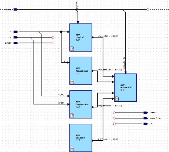
In addition to connecting existing signals and busses to the new blocks, we
must also create some internal signals and busses to connect some of the blocks
to each other. Use the Add Bus tool to add a new bus connecting the right
side of the Logical block to the left side of the Mux4Bus32
block. Rename this bus LogicalR and change it to type std_logic_vector(31 DOWNTO 0).
You should see the new bus appear in the declarations. This is now an internal signal,
analogous to a local variable in C, which only has meaning within this particular design
unit. Create similar signals connecting the other three operation class blocks to the
multiplexor called: ArithmeticR, ComparisonR, and ShifterR
respectively. Your block diagram should now look like the figure below:
Finally, follow the procedures which you have just learned to add busses and
signals so that your block diagram resembles the figure below:
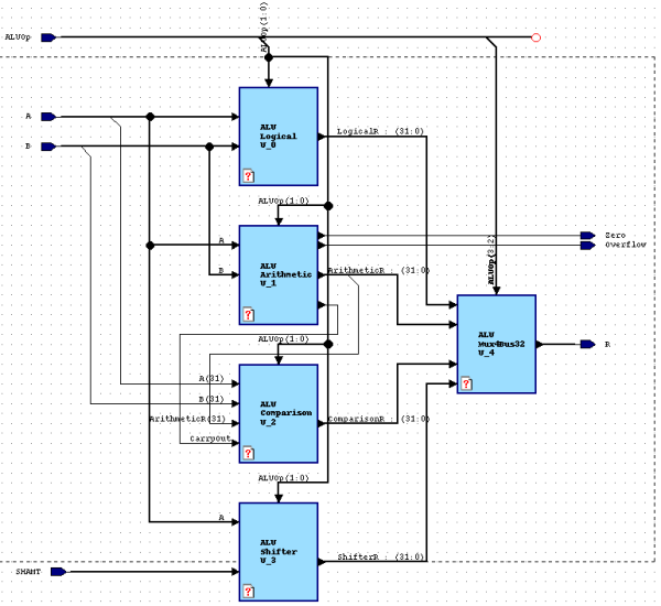
Feel free to try and make your design look cleaner looking. Once you are complete...
Creating the Logical sub-block