The first step in defining the Logical sub-block is to create a new view for it. This will create a new hierarchichal level of design files and allow you to define the behavior of this sub-block with one of the standard FPGA Advantage view: block-diagram, flowchart, state machine, truth table, or VHDL Text.
For the Logical sub-block we will be creating a new
block-diagram view. This is done by positioning the pointer
over the blue rectangle representing the block and right-clicking
to bring up the pop-up menu. From this menu, at the top,
highlight the Open As item and from the sub-menu
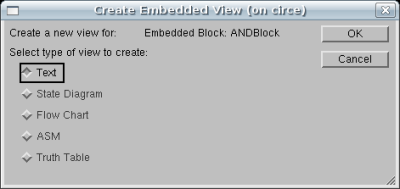
select New View. A window will appear asking you what
type of view you want to create. Select block diagram view
from the list click Next and then click Finish.
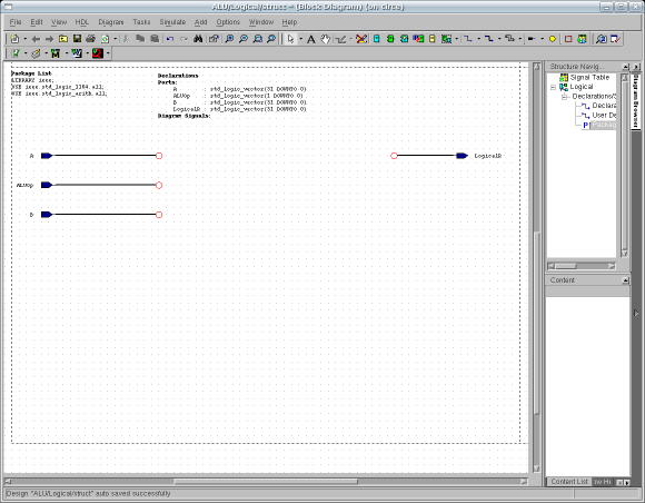
A new design window should appear resembling the figure shown below.
Notice that there are already input and output ports and busses placed
on the design. This is because the design unit symbol, the blue
rectangle on the parent design, already has signals connected to
it. These signals connected to the outside of the symbol are
automatically reflected by ports inside the design unit.
The logical unit will perform one of four operations:
AND, OR, XOR, or NOR. Each of
these operations will be performed in parallel on the inputs
and the output will be selected by a 32-bit wide 4-1 mux
controlled by the ALUOp(1 downto 0) signals. The encodings
for the operations are in this table:
| Operation | ALUOp(1) | ALUOp(0) |
|---|---|---|
| AND | 0 | 0 |
| OR | 0 | 1 |
| XOR | 1 | 0 |
| NOR | 1 | 1 |
There are many different ways in which this functionality could be implemented. What we will be doing is using embedded blocks to place fragments of VHDL code into the block diagram which will perform the important logical operations.
First, select the embedded block tool from the toolbar
by pressing the  button. Then
position the pointer over the block diagram between the input and
output ports and left-click to place an embedded block.
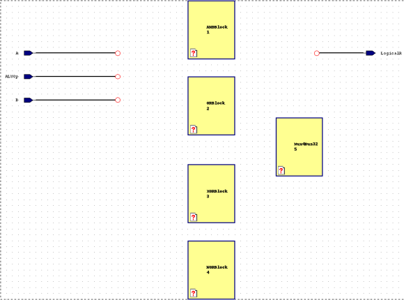
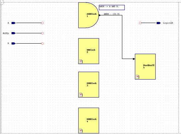
The embedded block appears as a yellow rectangle. Place
five embedded blocks on the diagram in the same manner that you
placed the sub-blocks in the top level block diagram. Label
the four columned blocks, from top to bottom: ANDBlock,
ORBlock, XORBlock, and NORBlock and the
other embedded block Mux4Bus32. Your design area should now
look like the figure below:
button. Then
position the pointer over the block diagram between the input and
output ports and left-click to place an embedded block.
The embedded block appears as a yellow rectangle. Place
five embedded blocks on the diagram in the same manner that you
placed the sub-blocks in the top level block diagram. Label
the four columned blocks, from top to bottom: ANDBlock,
ORBlock, XORBlock, and NORBlock and the
other embedded block Mux4Bus32. Your design area should now
look like the figure below:
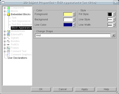
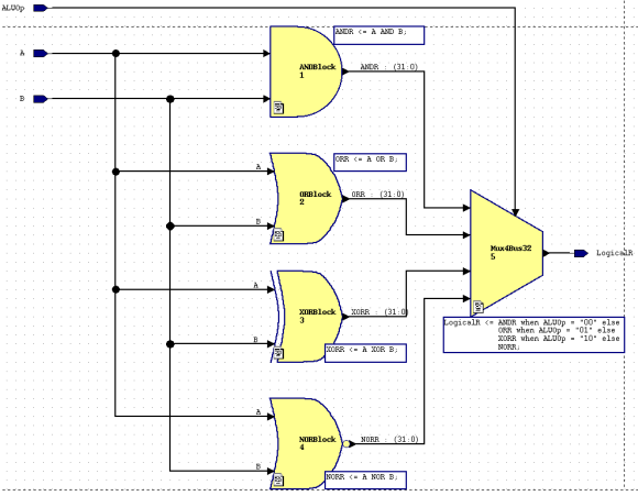
For cosmetic purposes, it would be nice to have our ANDBlock represented
by a symbol which resembles an AND gate. FPGA Advantage has a small number of
alternative shapes for blocks. To change the shape, right-click over the
ANDBlock block. At the bottom of the pop-up menu will be an option
called Object Properties. Select this option with a left-click. From the window
which appears, click the Block Appearance and select the desired
shape from list box.
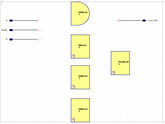
Click OK and your design should look like the figure below:
Embedded blocks will place fragments of VHDL code at the top level of the
architecture description for the current block. Generally we will be using
them to place what are called Concurrent Assignmet Statments
which will perform simple operations on data. Since the embedded
block VHDL code will be at the top level architecture for the view,
all of the signals in that view are automatically visible to the
embedded block and it is not necessary to actually connect
signals to them.
For ease of reading, we will connect the input and output signals
to the blocks. So, connect the A and B busses to the left side of
our ANDBlock. You may also wish to resize the block to make
it a little bit smaller. Then create a new bus from the output (right)
side of the ANDBlock called ANDR and connect it to the
input side of the Mux4Bus32 block.
Finally, we must tell the embedded block what to do. The VHDL code which
will Bitwise-AND two std_logic_vectors of the same size together is:
"ANDR <= A AND B;". To enter this code for the block, double-click the embedded
block and make sure Text is selected in the Create Embedded View windows.
Click OK.
An outlined box will appear anchored to the ANDBlock embedded block.
Highlight the text in this box and replace it with the VHDL code
ANDR <= A AND B;. You can resize and reposition the text as you like.
Your block diagram should now resemble the figure below:
Now finish the block diagram by changing the shapes of the OR, XOR,
and MUX blocks. There is no NOR symbol, so we can just use an
OR symbol with a bubble on the output. Do this by right-clicking
on the output port and turning Not | On.
Complete this by giving them the following embedded text:
| ORBlock: | ORR <= A OR B; |
|---|---|
| XORBlock: | XORR <= A XOR B; |
| NORBlock: | NORR <= A NOR B; |
| Mux4B32: | LogicalR <= ANDR when ALUOp = "00" else ORR when ALUOp = "01" else XORR when ALUOp = "10" else NORR; |
Your final block diagram should appear as the figure below. Save this
block and generate and examine the VHDL code for it.
You have now completely specified the behavior of the Logical
sub-block of the ALU. However, we do not yet know if it works
correctly. In order to determine this, we will start with an introduction
to the ModelSim simulator in Simulating the Logical Sub-Block.