The Design Manager, as you will discover, is the heart of HDL Designer and the location from which your design hierarchy is managed. Your design will be entered as a series of Design Elements which will have distinct names and will appear under the library name tree in the Design Manager window. Each design element will have a symbol and one or more Views associated with it.
The symbol will be the "Black Box" description of the design element
which describes its Input and Output interface. It will be used to generate
the Entity Declaration in the VHDL code and to create an instance of the
design element within a block diagram at a higher level of hierarchy.
A View is a description of the behavior of a Design Element.
In FPGA Advantage, a design element's behavior may be represented by a
Block Diagram View, a Flow Chart View, a State Machine
View, a Truth Table View, or an HDL View. The View
will be used to generate the architecture declaration in the VHDL code.
As in normal VHDL coding, a design element may be instantiated as a
component in another design element, creating a hierarchy. Multiple views
may be created for a single design element which may describe it in different
ways. When the design is generated into HDL, a single view must be selected
to describe the design element when multiple descriptions are available.
The first step in the creation of our ALU will be to create a
top level block diagram. A block diagram is very similar to a schematic
design: it contains symbols for design elements and I/O ports which are
connected by signals and busses. It will, however, contain several other
elements which allow the generation of complete, readable, and portable
HDL code instead of the proprietary wirelist files generated by schematics
tools.
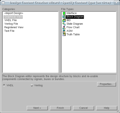
To create a new Block Diagram View go to the File | New |
Design Content menu of the Design Manager. Make sure the
"Graphical View" category is selected in the left pane and select
Block Diagram from the right and click Finish.
This will bring up the window seen below:
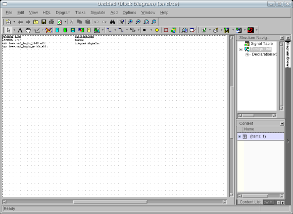
Before we start, notice the two text blocks labeled Package List
and Declarations at the top of the design area. These two lists
will be automatically updated with information which will be used to properly
generate the HDL code for your block diagram.
We will start by placing symbols on the block diagram to represent the
I/O ports with nets/busses attached to them: