This sequence of tutorials will guide you through the creation of a digital standard cell library.
The first you thing you need to do is get a copy of the cds.lib file, which will be your initial library mappings file. This file points Cadence to the technology libraries for the AMI C5N process.
Copy "cds.lib" into your Cadence working directory from ~jbakos/cds_work.
Next, start up the Cadence IC-Tools from your Cadence IC-Tools work directory using the command "icfb".
Once you do this, you should see a "what's new window", the command interface window (CIW), and the Library Manager. Close the "what's new window".
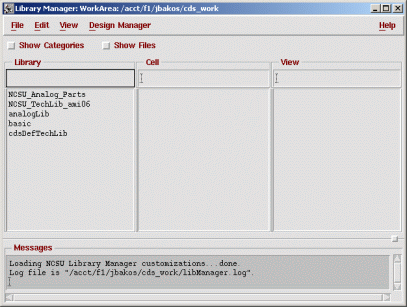
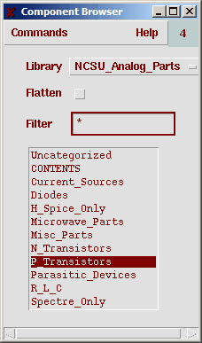
First, check your Library Manager window to verify that you have all of the necessary libraries available in your Library Manager. If so, it should look like this:
If you don't see all of these libraries, you might not have started icfb in your Cadence working directory or your cds.lib file might not be present in your Cadence working directory. If you need help, contact the instructor.
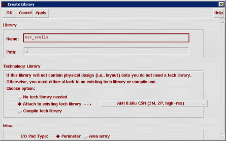
Now let's create a new library for our cells. We'll call this library "usc_scells". In the Library Manager, select File | New | Library. Type "usc_scells" for the library name and "." for the path. Note: a subdirectory named after the library will be created under the path you specify. Select "Attach to existing tech library" and select "AMI 0.60u C5N (3M, 2P, high-res)". Click OK.
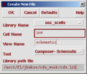
Now let's create an inverter cell. In the Library Manager, select the usc_scells library, then select File | New | Cell View. The library name should be "usc_scells." For the cell name, type "inv". The view name should be "schematic", and the tool should be "Composer-Schematic". Click OK.
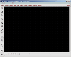
You will now see a Virtuoso schematic editor window.
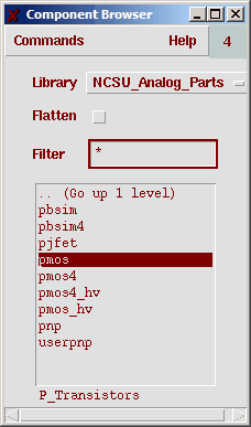
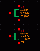
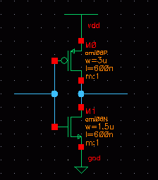
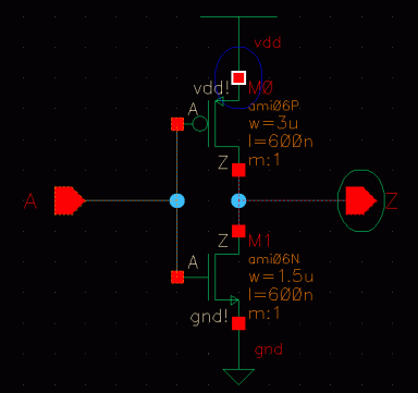
In the schematic editor, there are only a few important commands you need to know. First, let's instance a PMOS FET from the NCSU design kit. To do this, press the I button on your keyboard. In the Component Browser window, make sure the Library "NCSU_Analog_Parts" is selected. Click "P_Transistors" in the list below. Then select the "pmos" cell and make sure the "symbol" view is selected in the Add Instance window.
The properties for this cell are shown in the instance window, but let's leave these alone for now. Go back to the schematic editor window and you'll notice that you are now in placement mode. Click your left mouse button to place the transistor somewhere in the schematic editor window, then press your Esc key to exit placement mode. You'll notice that the placed PMOS cell has a subset of its properties shown in the schematic window.
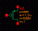
"M0" is the instance name and "ami06P" is the name of the simulator model associated with this FET. Now, recall that channel geometry is the most important parameter for MOSFETs. The width and length of the channel (or gate) defines (among other things) the transistor size, switching speed, current, and input capacitance. In the schematic window, "w=1.5u" defines the channel width, which was set by default to 5 * lambda. "l=600n" defines the channel length, which is set by default to the minimum channel size (equal to minimum feature size) for the process. "m=1" defines the multiplicity, which is a way to construct transistor structures with large effective widths by simply using multiple transistors in parallel.
Typically, high-speed digital logic cells are formed with MOSFETs having minimum process channel length, but the width is set according to the characteristics you want for the transistor. Remember that each input to a logic cell is usually fanned out to two transistor gates, so the total input capacitance will increase by a factor of 2 as your increase the widths of the transistors (actually more than a factor of two, since PMOS's usually have twice the channel area of NMOS's). On the other hand, transistors with larger widths draw more current and switch faster. Let's leave the width set to 1.5 um (5 lambda).
Now let's check out ALL the PMOS parameters. Click the PMOS to highlight it, then press the
Q button, which brings up the properties window for any selected design object. You will see the following window.
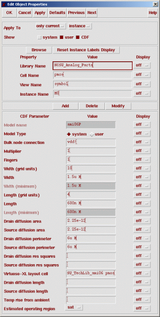
Notice that the bulk terminal is set to be implicitly connected to vdd!, which is a special global net used in simulation to represent the power supply. The source and drain diffusion area/perimeter values will be updated automatically if you change the length or width of the channel.
For the NCSU design kit, the channel width and length can only be set to values that are an integral multiple of grid units, and a grid unit is .15u (150 nm). This grid unit was set to be half lambda. The properties page allows you to specify/express width and length as either a real value or as a multiple of grid units.
Now let's add an NMOS in a similar manner.
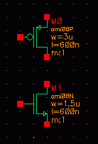
Notice the default width of the NMOS is also 1.5um. Recall that PMOS's should always be about twice the width of the corresponding NMOS in order for rise time to match fall time (because holes have about half the mobility of electrons). Therefore, let's double the width of the PMOS to 3um. Do this by selecting the PMOS, hitting the Q key, changing the width to "3u", and clicking OK.
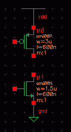
Now let's add two special cells that are used to make any net they are connected to become either the global power (vdd!) or global ground (gnd!) nets. Note that any net name followed by a ! becomes a global net, which exists across of the entire design hierarchy. These special symbols are found in the "analogLib" library. To add them, press I, select the "analogLib" library in the Component Browser window, select Sources, Globals and then vdd. Place the T-shaped symbol such that it connects to the drain of the PMOS. Repeat this step with the gnd symbol, but connect it to the source of the NMOS.
Now let's wire it up the circuit. Use the wire button...
...to connect the source of the PMOS to the drain of the NMOS. Add an additional wire stub for the output. Connect the PMOS and NMOS gates and wire up an stub wire for the input. Press the ESCAPE key to exit wire-mode.
Now let's add an input pin and an output pin. Click the pin button...

...enter "A" for the name, make sure the direction is set to input, and turn off "attach net expression".
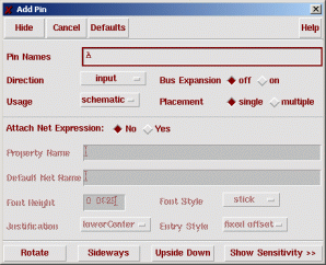
Place the input pin on the input wire. Repeat this procedure to add an output pin named "Z" to the output wire. Make sure the direction for the second pin is set to output. Note that adding pins to wires has a side effect of assigning the pin name to the the corresponding wire/net. This is similar to what happens when you addded the special power supply symbols. Now every net in our design has a name, meaning that the editor did not have to automatically assign net names to any wires. Sometimes you will need to assign a name to a net/wire that isn't connected to a pin or supply. This will be useful when you want to plot a voltage involving an internal wire. To do this, simply use the wire name button:

Other essential commands are delete (delete key), undo (U key), copy (C key), and move (M key, although you can click-drag components as well). When placing and explicitly moving components, the right mouse button will perform a 90-degree rotate. You can select/highlight multiple components by holding down the shift key and clicking, or by drawing a box with your mouse. Use the Z key to zoom in on an area that you draw with your mouse, control-Z to zoom in without needing to draw a zoom box, shift-Z to zoom out, and the F key to fit the entire design to the window.
Also, notice that Virtuoso has a peculiar way in which commands are executed. For example, regardless if you have a component highlighted when you hit the C key, you still need to click inside the editor window before you actually copy the component. The location where you click becomes the "reference point" for your mouse cursor. As always, you need to hit your escape key to stop repeating the same operation over and over. You'll get accustomed to this with time. I recommend that you take some time now to experiment with the editor.
Your design should now look like this:

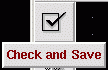
Save your design using the "check and save" button...
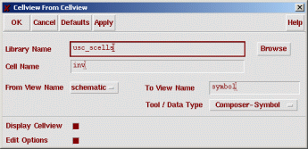
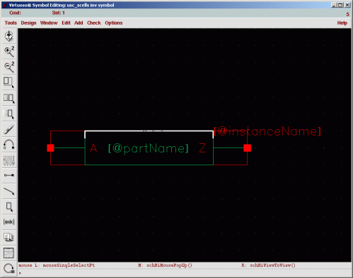
Now let's create a symbol view for the inverter, so you can instance this cell in other designs. Select Design | Create Cellview | From Cellview. Click OK on the resultant window.
You will now get a new Virtuoso window with an automatically generated symbol. This is simply a symbol editor.
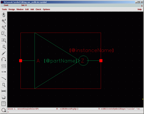
Play around with the various editor features to change this into a "real" inverter symbol. Put your artistic talents to work and see if you can design a better-looking inverter symbol than I could!
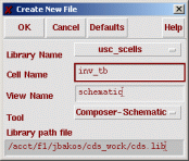
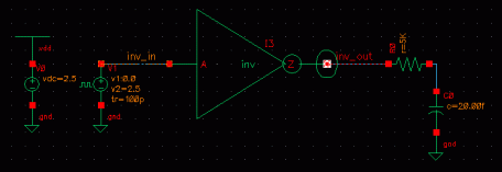
Save your symbol and close your editor windows. Now we need to simulate our inverter. The basic idea here is that we can simulate a schematic design, but to do this, we need to add a power supply, an input stimulous, and some kind of load for the inverter to drive. These components are really parts of a "test bench" but we don't want to include these directly into our inverter design. This is because after testing, we'll need to use our inverter as part of a larger design and we will no longer want or need these "testing" components in our design. To solve this problem, let's create a new schematic for our test bench, and add the inverter to this schematic as another testing component. So go back to the Library Manager and create a new schematic cell called "inv_tb".
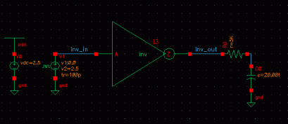
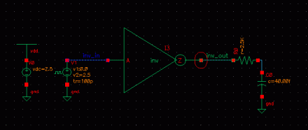
Let's instance our inverter (using the I button), along with a DC source (vdc), a pulse source (vpulse) and an RC load (to simulate a realistic output load). These components can all be found in "analogLib" Library. Wire these components up as shown. Notice that I named the input and output wires to the inverter.
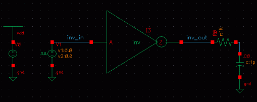
Now let's assign properties to these components (by selecting and using the Q key). Set the supply DC voltage to "2.5" (don't include V as the units, this is assumed). Set the pulse-source such that voltage 1 is 0, voltage 2 is 2.5, rise and fall times both to "100p", pulse width to "10n" (corresponding to a input switching rate of 100 MHz), and period to "20n".
Note: when testing more complex logic gates, you can use a vpulse sources for each input. The pulses may be setup to have widths (duty cycle) and periods that are multiples of each other. For example, when testing a 2-input NAND gate, use two vpulses with duty cycles and period of 10n, 20n and 20n, 40n respectively. Using this technique, you can easily set up testbenches that cycle through all input combinations. You can also make use of the "delay" parameter to offset the first rising or falling edge of certain inputs.
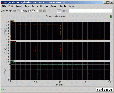
For example, here's a sample simulation waveform for the D-flip-flop.
Set the load resistance to "5K" and the load capacitance to ".02p". Your design show now look like this:
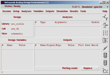
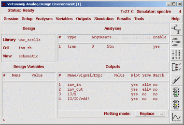
We're now ready to simulate! Save your design, then select Tools | Analog Environment to start up Spectre, the Cadence version of SPICE. Close the annoying "what's new" window. The Spectre window will be shown.
In order to simulate our design, we'll first need to specify an include file which defines a set of process fabrication characteristics (such as oxide thickness, doping, etc.) for the NMOS and PMOS devices. These characteristics are called device models.
Fabrication processes, like everything else in the world, are not perfect. In fact, the exact characteristics of the features on a chip have inherent variations that occur during fabrication (within certain tolerances). These process variations result in a range of performance of each NMOS and PMOS, which affects switching speed, current, power consumption, etc.
As a result, many design kits encapsulate this range of performance characteristics using a set of three models for both the PMOS and NMOS. These models are called "nominal (or typical)," "fast," and "slow." When simulating a design for the purposes of design timing verification, if the circuit is performing very close to the design requirements then testers will quit using the "nominal" models and instead use "corner testing," which is when you perform simulations with the four combinations of models using the FAST and SLOW versions of the NMOS and PMOS models.
In other words, NMOS and PMOS models usually come as a set of 5 configurations. The first configuration is where the PMOS and NMOS have "nominal" performance and the other four configurations are:
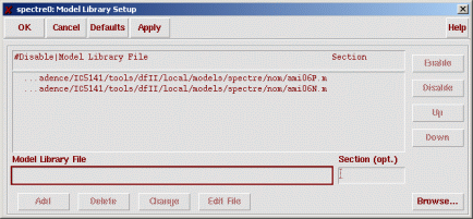
Let's use the nominal models for now. To setup our models, select Setup | Model Libraries. For the model library name, type "/usr/local/3rdparty/cadence/IC5141/tools/dfII/local/models/spectre/nom/ami06P.m" for the PMOS model and click Add. Now type "/usr/local/3rdparty/cadence/IC5141/tools/dfII/local/models/spectre/nom/ami06N.m" for the NMOS model and click Add. Click OK.
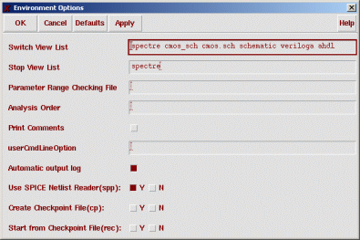
Also, because the NCSU CDK only has SPICE-formatted MOSFET models, we need to tell Spectre to accept these models. To do this, select Setup | Environment. In the window, turn on "Use SPICE Netlist Reader (spp)".
Now let's select the type of simulation we'd like to run. There are various types of analyses we can perform, but let's choose a transient (time-domain) analysis. Click the "Choose Analyses" button.
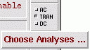
In the window, select "tran" and specify "50n" as the stop time. Recall that our input data rate is 100 MHz, so this time will allow us to see 5 bits entering our inverter. Click OK.
Now let's select voltages and currents to plot for our simulation. Select Outputs | To Be Plotted | Select On Schematic. A schematic window will pop up. Clicking wires will display the voltage of the corresponding net, while clicking pins will display the current for the corresponding component and net.
Click the wire called "inv_in" and the wire called "inv_out". This will show us the input and output voltage of the inverter. Now suppose we want to plot total current that is drawn from the inverter output pin. Click the output pin of the inverter. Now let's suppose we want to see the current that is being drawn by the PMOS transistor within the inverter. However, this will illustrate how we can select internal nets/pins within a lower-level of design hierarchy.
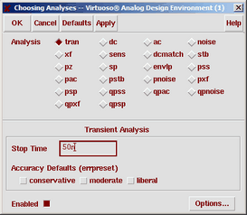
To do this, press the X key, which does a "descend read" (shift-X does a "descend edit"). Now click the inverter. You'll see the following window.
Click OK to open a schematic of the inverter. Now click the drain of the PMOS. You should now see the following window.
Now let's go back up to the testbench level of the hierarchy. Press the B key to return to the top. Your window should now look like the following.
Press the Esc key to exit the mode for selecting outputs. Go back to your Spectre window and you should now see the following.
Now let's generate a netlist for our design. Select Simulation | Netlist | Create. You'll see the following netlist.
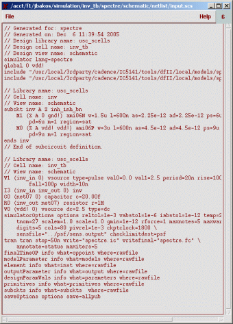
It's important to become familiar with how netlists are organized and represented, because sometimes the netlist can be used to debug your design.
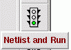
Now close this window. It's time to simulate. Click the "Netlist and Run" button.
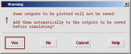
You'll get a window that says that some of the outputs to be plotted will not be written to the output file. This is because the saveOptions simulator command instructs the simulator to only saves voltages, but we have currents in our output list. Click YES on this window.
If you get a "Welcome to Spectre" window, close it by clicking OK. You should also see a simulator output window and a waveform window. Before we look at those, notice the error message about /I3/I0/vdd!...
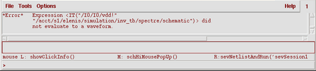
You're getting this window because of a bizarre bug in Cadence. We can fix this by going back and re-adding that pin to the output list. Go back to the Spectre window, select Outputs | To Be Plotted | Select on Schematic. On the schematic window, hit the X key and click the inverter again to do a "descent read". In the inverter design, click the PMOS drain once to make the ellipse disappear, then again to make it reappear as a different color. Now hit your Esc key. If you go back to the Spectre window, you'll notice a new output listed in the output window. This is the same pin, but references the PMOS instance as M0 instead of I3. Your window shold look like the following.
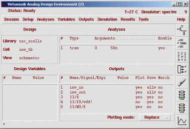
Click the I3/I0/vdd! output and delete it from the output listing using the delete button.

Now click the netlist and run button again. You will again review the following window.
Again click Yes. Now the PMOS drain current is shown on the waveform plot. You should see the following waveform window.
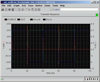
All the traces are overlapped on a single plot. Let's separate those plots by selecting Axis | Strips. You should now see the following window.
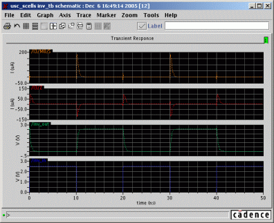
By observing inv_in and inv_out, you'll notice that the inverter is indeed doing exactly what it's supposed to be doing: logically inverting the input. You'll notice current spikes on /I3/M0/S, representing the dynamic switching current being drawn from the power supply by the PMOS. Dynamic current occurs as a result of the PMOS and NMOS simultaneously transitioning through their linear region. You'll also notice dynamic current being sourced and sinked at I3/Z, which is the output of the inverter. These two current values aren't equal, since the total current being drawn through the PMOS is being split between the output path and the NMOS path.
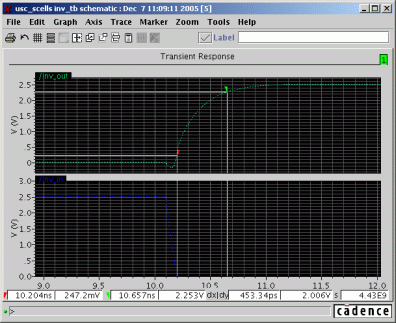
For now, let's delete the two current plots. You can do this by clicking each plot and hitting your Delete key. Now let's take a closer look at the voltage output of the inverter. Hit your Z button, and draw a zoom box tightly around the first rising edge of inv_out. Don't worry if you make a mistake. You can always use your F button to zoom back out such that the entire plot is shown and try the zoom again.
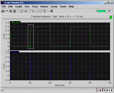
After zooming, your plot should look like the following.
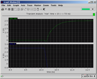
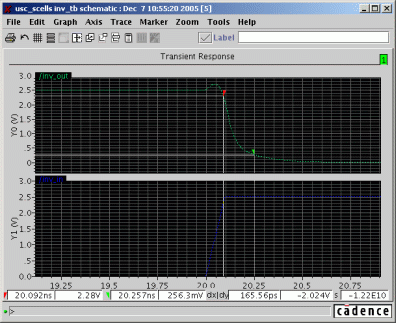
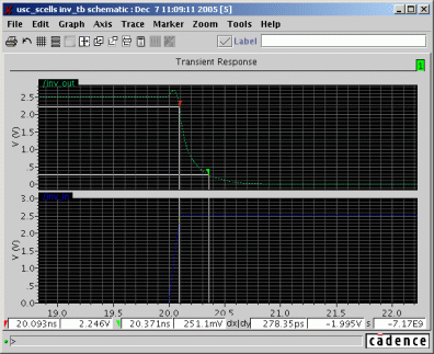
Let's measure the approximate rise time of the inverter. To do this, turn on your delta cursor by hitting your D key. Move the red cursor (by dragging the red triangle) to the point at which the output begins to rise. For our approximatation, this should be when the output is 10% of the full voltage swing, or about 250 mV. Likewise, move the green cursor to the point at which the output is 90% of the full swing voltage, or about 2.250 V. Your plot should look like the following.
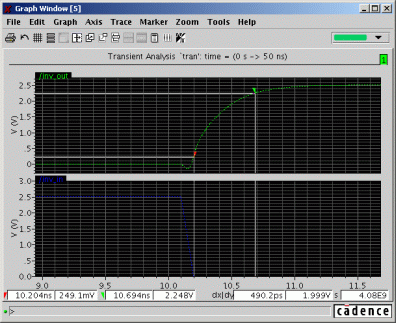
You can see at the bottom of the window that the rise time (time difference between the two cursors) is approximately 490.2 ps.
Let's do the same for the fall time. Hit your F key and zoom into the first falling edge of inv_out. Position your delta cursors at 2.250 V and 250 mV.
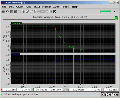
The fall time is approximately 621.99 ps. Looks like the NMOS is having more trouble pulling the output down than the PMOS has pulling the output up.
Let's check out how much current the inverter is drawing. Close your waveform window and tell Spectre to replot the outputs by clicking the "plot outputs button."

Note: another way to do this would be to select Results | Direct Plot | Transient Signal, then click on the net or pin you wish to plot. This is useful in situations where you're debugging a circuit and wish to quickly probe voltages or currents that are NOT listed in your "outputs list". Just remember that you can only do this for voltages and currents that were saved to the output file during simulation. By default, all voltages are saved but currents are not. You can change these settings by selecting Outputs | Save All. If you need to plot a signal that was not saved during simulation, you will need to either add that signal to the "outputs to be saved" list or adjust the "Save All..." settings, then resimulate.
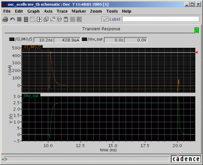
Now turn off your delta cursor (if it's still on) using the D key. Delete all the waves except for /I3/M0/S and inv_out. Recall that the /I3/M0/S pin represents the current that's being drawn from the power supply to the PMOS in the inverter. For this design, this PMOS is the only component that is connected to Vdd and thus the current through this pin represents the total supply current requirement for the entire circuit. However, for more complex designs where multiple PMOSs are connected in parallel to Vdd, we can still measure total current draw by plotting the current through one of the pins on the global power supply (DC source).
Zoom in around one of the output bit times (including one rising transition and one falling transition). Activate the horizontal cursor by hitting your H key, and move the cursor (by dragging the red arrow) to the maximum point on the current plot. As you can see, the maximum dynamic current draw occurs on the rising edge of the output, which is when the PMOS is pulling up.

The current is approximately 177.8 uA (you may get a slightly different value due to zoom level). This yields a maximum instantaneous dynamic power consumption of 2.5 V * 177.8 uA = 444.5 uW (microwatts). To put things in perspective, assume we have an entire chip containing 10 million of these inverters. Assume every transistor pulls its output up simultaneously (which is not likely). The total instantaneous power consumption would be (444.5 * 10^-6) * (10^7) = 4450 watts! Yikes! Good thing this was such a contrived and unlikely example!
Note that you can also use the trace cursor (by hitting your C key) to check out the static current when the PMOS is not switching.
In conclusion, this inverter, driving a capacitive load of 20 fF and resistive load of 5K ohms, with a really clean input signal having 100 ps rise and fall times, needs at least 630 ps (~490 to 0->1, ~620 to 1->0) to transition. Let's see if we can improve on this.
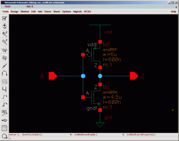
Go back to your Library Manager and open the inverter schematic. Let's increase the width of the PMOS to 6 um, and increase the width of the NMOS to 4.5 um. In other words, we doubled the width of the PMOS, but we multipled the width of the NMOS by 3 (in order to compensate for the weak pull-down).
Save your design, go back to Spectre, and click the "netlist and run" button. Now let's measure our rise time and fall time...
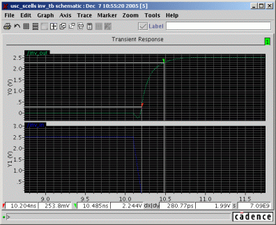
The new rise time is 280.77 ps and the new fall time is 165.56 ps. The rise and fall times have been about halved, but now the NMOS is pulling down faster than the PMOS is pulling up. The tables have been turned! Unfortunately, the circuit is still not balanced. As you can imagine, manually tweaking transistor sizes to balance rise and fall times is not feasible. Cadence provides a tool called Neolinear which automates this process.
Also, observe the new current draw from the power supply using /I3/M0/S. The current is now 438.9 uA.
Now that we have a fast inverter, let's dertermine the effect of doubling the output load. Open the testbench design and increase the capacitance to 40 fF and decrease the resistance to 2.5 K ohms. Save the design, rerun the simulation, and measure rise and fall times.
As you can see, the rise time has increased to 453.34 ps and the fall time has increased to 278.35 ps. The inverter's speed depends on the output load! This modeled output load represents inputs of other logic gates that this gate is driving. So, for example, when we the output load was 20 fF/5K ohms, the inverter may have been driving 2 gates (fanout of 2), but when the output load was 40 fF/5 ohms, the inverter may have been driving 4 gates (fanout of 4).
Here's a table of what we've measured.
| PMOS width | NMOS width | Cap. load | Res. load | Rise time | Fall time | Ins. dyn. current |
|---|---|---|---|---|---|---|
| 3 um | 1.5 um | 20 fF | 5 Kohm | 490.2 ps | 621.99 ps | 177.8 uA |
| 6 um | 4.5 um | 20 fF | 5 Kohm | 280.77 ps | 165.56 ps | 438.9 uA | 6 um | 4.5 um | 40 fF | 2.5 Kohm | 453.34 ps | 278.35 ps |
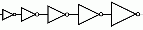
You can see now why most logic cell libraries have several different versions of each gate, each made of transistors with different sizes (usually a 1X, 2X, and 4X).
Smaller gates have low input capacitance (they're easy to drive) and low power dynamic consumption, but they have low drive strength (are used for low fanouts). Larger inverters have high drive strength (are used for higher fanouts), but high input capacitace and they consume significantly more power. Given equal output load, larger gates will switch faster. For a fixed switching time, larger gates can drive more load.
In order to drive a large fanout or highly loaded net, a large gate must be used. But a weak signal cannot drive the input of such a large gate, so a medium sized gate is used to drive the large gate. This techique is referred to as a tapered inverter chain.
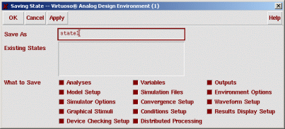
Before you close Spectre, let's save the state of our simulation environment. This will save the model paths, outputs, etc. Go to Session | Save State and click OK.
That's all for this tutorial. Next I'll show you how to perform layout, LVS, DRC, and extraction!