This tutorial will guide you through the layout of your inverter cell.
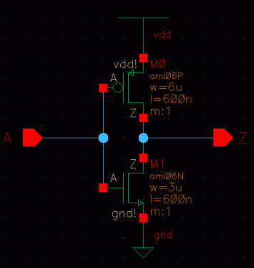
First, open your inverter schematic. Let's set the width of the PMOS to be 6u (20 lambda) and the width of the NMOS to be 3u (10 lambda).
Now's let's enter layout mode. Select Tools | Design Synthesis | Layout XL. In the following window, select "Create New".
In the next window, click OK.

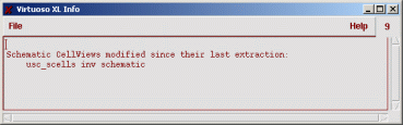
If you see the following window, close it and save your inverter schematic using the "check and save" button. This will "extract" your schematic design.
You may also see a "what's new" window. If so, curse at Cadence and close the window.
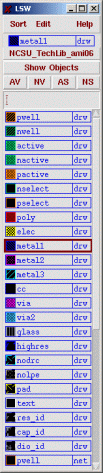
You will now see three windows. The first is your schematic window, the second is the layout editor window, and the third is the layer picker window (LSW), which displays all the available layers in the AMI C5N process. You can also use this window to make certain layers invisible (after a refresh of the editor window) or non-selectable.
Note: the layout editor is now in "Layout-XL" mode. In this mode, your layout editor is linked to the schematic for your design. This keeps the instance names of all your instanced cells (FETs) consistant between the layout and schematic. This is absolutely essential in order to get the LVS checker (Layout vs. Schematic) to work. As such, you need to make sure that all your layout work is performed in the Layout-XL tool.
Once you create a new layout view using the "Design Synthesis" command in the schematic editor, you may need to reopen your layout in a later session to continue your layout work. To do this, you can first open the layout view in the Library Manager. However, before you begin work, you'll need to re-enter "Layout-XL" mode. In the layout editor window, you can do this by selecting Tools | Layout-XL.
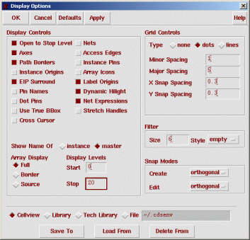
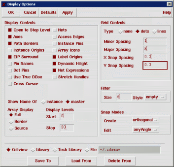
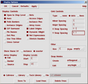
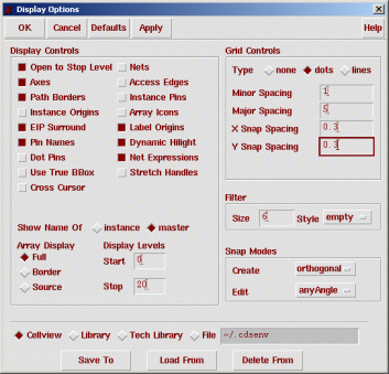
Before we start drawing layout, we need to make a change to the layout editor options. The current snap grid is set to .15 um (.5 lambda) by default. This setting is fine for doing most of your layout work. However, there appears to be a design rule for the technology library that requires that your MOSFETs be placed on a .3 um (lambda) grid. As a result, at this point we need to set the grid to .3 um. To do this, select Options | Display. Set the X snap spacing and Y snap spacing to .3. Click "Save To", then OK. Note that "Save To" only saves the display options for whatever view you're currently editing.

The first thing we should do is draw our power rails. This means that we have an important decision to make. How tall should we make our cells? Whatever value we use, we'll need to keep this consistent for all our cells such that they can be snapped together. Let's go with 40.5 microns, which should give us adequate room for routing within our cells (and it's a multiple of our grid spacing). Note: this decision was also motivated by the fact that we'll want a 4.5 um grid for pins and routing in place-and-route. 4.5 um is a nice number, as it is an even multiple of lambda as well as the minimum width and spacing of all three metal layers.
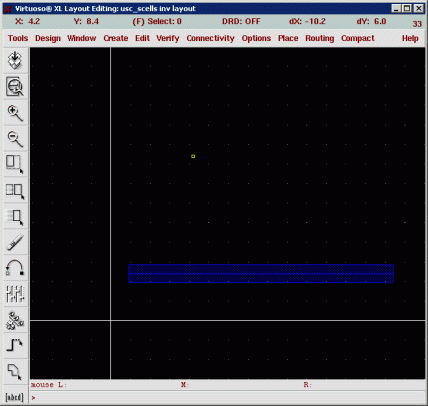
Let's start out by drawing a metal1 wire for our ground rail. In the layer picker window, click metal1.
In the layout editor, press the P key to draw a path, and draw a wire starting near the origin. For the moment, make the wire 13.5 microns long. You can check the length by watching the dX measurement at the top of the editor window. Double-click to end the wire and press the Esc key to end path mode.
Note that once we finish placing our MOSFETs, you might need to go back and change the length of the power rails.
Recall that you can use the the zoom commands (Z key to draw a zoom box, control-Z to zoom in, shift-Z to zoom out) and pan (using the arrow keys) to get a better view of the wire. You might need to experiment with the zoom level in order to precisely draw your wire.
By default the metal1 wire is .9 um wide, which is the minimum width. In order to make sure our supply rails can supply sufficient current to our circuits (and to reduce supply noise), we should use a much thicker wire for the supply rails. Let's increase the width to 3.6 um. Click the wire, press Q to bring up the properties, and change the width to 3.6.

Now let's move the wire such that the lower-left corner is at the origin. Select and drag the wire such that the left edge touches the 0-point on the X-axis. Notice the editor is current in orthogonal-move mode. We can change this, but we'll wait until later. Now move the wire down such that the bottom touches the 0-point on the Y-axis. You may have to zoom in tight in order to verify that the wire is touching the axis.
Now let's draw our Vdd rail. We want it to start at 0 on the X axis, be 13.5 microns long, 3.6 microns wide, and the top edge to be at 40.5 on the Y axis. The center point would be at Y coordinate 40.5 - 3.6/2 = 38.7. Zoom out such that the editor window spans the Y axis up through 38.7. You will know this by moving your mouse point around and watching the X and Y position values in the top-left corner of the editor window. Once your zoom level is good, hit your P key, position the cursor at (0,38.7), and draw a 13.5 micron long wire (you'll know the length by observing the dX at the top of the window). If you find this difficult to do, you can always zoom in, zoom out, and pan while you're drawing the wire.
Once you do this, change the wire properties to make the width 3.6. After you do this, make liberal use of the zoom commands while moving your cursor and watching the (X,Y) coordinates to verify that the Vdd rail has its left edge at X-coordinate 0, its top edge at Y-coordinate 40.5, and its right edge at X-coordinate 13.5. After you verify this, press your F key to fit everything to the window.
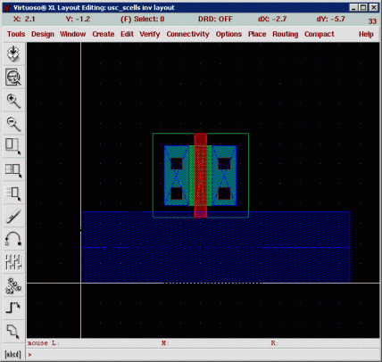
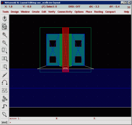
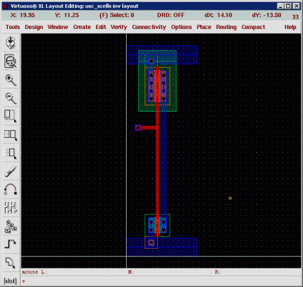
Now let's add our NMOS to the design. To do this, select Create | Pick From Schematic. Go over to the schematic window, click the NMOS, go back to the layout window, and place the NMOS very near the ground rail. Hit Esc to quit place mode.
We can't see anything inside the NMOS cell (just a red border), so let's change that. In the layout editor, select Options | Display. Under "Display Levels," change "Stop" to "20" and click OK. Note that you may also want to turn on "Cross Cursor," which explicitly shows the X and Y locations of your cursor with a window-sized cross hair. This is a personal preference, so turn it on if you are comfortable with it. Click "Save To", then OK. We can now see the internal layout of the NMOS.
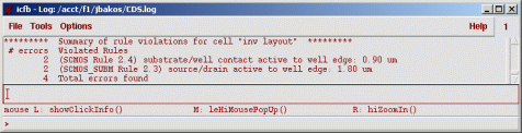
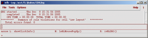
I put the NMOS very close to the ground rail, so I could maximize the space inside the cell for routing. However, there is metal1 contained with the NMOS on the source and drain. There is a possibility that I have violated the metal1-to-metal1 design rule. Let's check. Go to Verify | DRC and click OK.
The results of the DRC run are displayed in the command interface window (CIW).

As you can see, the metal1 in the NMOS must be at least .9 um from the ground rail. Move the NMOS such that the metal1 in the NMOS is .9 um away from the ground rail (the bottom edge of the metal1 in the NMOS should be at Y coordinate 3.6 + .9 = 4.5). There's a trick in doing this. Highlight the NMOS, hit your M key to enter move mode, then click the button edge of the metal1 in the NMOS (the bottom of the source or the drain). This way, the reference point for the move is the same edge that you're positioning. When the Y coordinate hits 4.5, click and you're done! Once you move the NMOS, rerun the DRC.
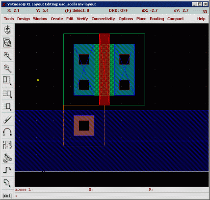
Now let's add the PMOS using the same method. In this case, don't worry about minimum spacing to the Vdd rail. You'll see why in a moment.
Recall that the PMOS has an n-well that forms the body terminal of the PMOS transistor. This body terminal must be tied to Vdd in order for the PMOS to function. The easiest way to do this is to move the PMOS such that the well (shown in the layout as a green rectangle) overlaps the Vdd rail. Then we can add a contact in the overlapping region such that the well is tied to Vdd. Recall that a contact is simply a hole in the silicon dioxide (glass) layer between the substrate and metal1 routing. This hole will allow metal1 to flow down through the hole in the oxide during the deposition process, which will form an electrical connection between the metal1 layer on top of the hole and the substrate (or well) beneath the hole.
In order to form a good electrical connection (i.e. low resistance) from metal1 to the n-well, we need to do more than just use a contact. We need to use an "ohmic" contact, which is a contact with a heavily-doped diffusion area underneath it. In other words, in order to form an ohmic contact with the n-well, we need a contact with a heavily-doped n diffusion area underneath. Recall that diffusion areas are always more heavily doped than the well or substrate silicon. Diffusion areas are also used for the source and drain of MOSFETs. Heavily n-doped silicon is referred to as "n+", whereas the well material is referred to as just "n". Such layers in layout editors is referred to as "n select" (and "p select").
Let's add the omhic contact. Hit your I key to add an instance. Browse to the NCSU_TechLib_ami06 library and select the "m1_n" cell (use the lowercase version). The "m1_n" cell is simply a square of contact layer ("cc") surrounded by a larger square of metal1, and around that an even larger square of n-select. Note: you can also just hit your O button to create a new contact. When you hit O, a window will appear allowing you to select which type of contact you'd like to instance.
The contact cells are designed such that they are automatically scalable while the base size satisfies all the design rules for:
Note that we could have drawn this contact ourselves (instead of using a cell), but doing this way is far easier.
Move the contact onto the Vdd rail, such that the bottom edge of the metal1 square meets the bottom edge of the Vdd rail. Before you do this, now would be a good time to turn off orthogonal move mode. Select Options | Display and change the "edit" snap mode from to "orthogonal" to "anyangle". Click "Save To", then OK. Now move the contact.
Now let's move the PMOS up such that the p-select (orange box) meets the the n-select (green box) of the contact cell.
Let's do a DRC check.
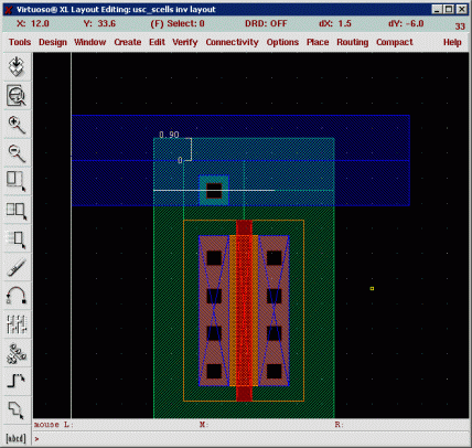
We got errors. The first error says that the well must extend past the n-select (contact active) by .9 um. Let's fix that. Let's use the ruler for this (bottom-most button on the layout editor -- you may need to resize your layout editor window to expose the button). Note that rulers do not affect the layout in any physical way. You can add rulers using the K key and clear the rulers by hitting shift-K. Draw a .9um ruler from the top edge of the n-select.

Now let's extend the n-well. Select the nwell layer in the layer picker, go back to the layout editor, and hit your R key to draw a rectangle of nwell up to the top of the ruler.
Now let's run another DRC.
No DRC violations.
Wait a second. After adding the contact, you can see that the contact layer is black. It appears that the PMOS has its own internal contacts. That is true, but these contacts connect the metal1 in the source and drain to the p-select in the substrate. To be precise, contacts will electrically connect the metal1 layer to whatever is beneath it. So the connection will depend on what layer is beneath the contact. This could be n-select, p-select, or polysilicon.
Okay, now that we're more familiar with the process design rules, let's make sure that the NMOS is down far enough that its internal metal1 is minimum-spaced to the ground rail. Remember, we're doing this to maximize the space inside the cell for routing (interconnect) area.
Move the NMOS down, closer to the ground rail.

Run a DRC check. You'll get the following errors.
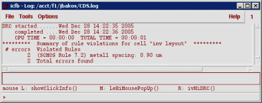
Let's use another ruler to move the NMOS such that its internal metal1 is .9 um from the rail. Note that the minimum metal1 spacing matches the metal1 minimum width. This is relatively common for poly and metal wires in fabrication processes. In this process, both the minimum width and spacing for metal1 and metal2 is .9 um. However, the minimum width for metal3 is 1.5 um while the minimum spacing remains at .9 um.

Now wait another second! Now we have the PMOS's body terminal connected to Vdd, how do we ensure that the NMOS's body terminal is connected to ground? Good question. The chip substrate in this process is doped with P material and this very same substrate material is used for the body of the NMOS's.
However, we still need to explicitly connect the chip substrate to ground. To do this, we can add another ohmic contact to the ground rail.
But wait, you ask. I know that the n-wells are isolated. Therefore each well must be connected to Vdd. However, the chip substrate is shared among all the NMOS's. Therefore, all I need to do is to have a single contact from ground to the substrate, and this will ground the entire substrate (and thus all the NMOS body terminals).
This is true. HOWEVER, you can never have too many substrate contacts. The more contacts, the tighter the connection and the less potential for noise. If we put a contact in all our cells, there will be at least one substrate tie-down for every cell on the chip. This is a lot of contacts. This is good. Now let's put in a contact.
To do this, instance a "m1_p" cell from the technology library (you can use your O key). Again, place the contact cell such that the p-select meets the n-select.
Okay, good. Now we need to tie the gates of both transistors together to form the input of the inverter. We'll do this with a poly wire. First, go back to Options | Display and make sure the "Create" mode is set to "orthogonal". Click "Save To" and then OK.
Select poly in the layer picker and draw a vertical wire the middle of the NMOS gate to the middle of the PMOS gate. Notice the wire width is .6 um, which matches the channel width as well as the minimum feature size for the process. Notice that Layout-XL will highlight in green the objects that share electrical connectivity with the net where you started the route. This will assist you in routing. Layout-XL obtained this information from the schematic.
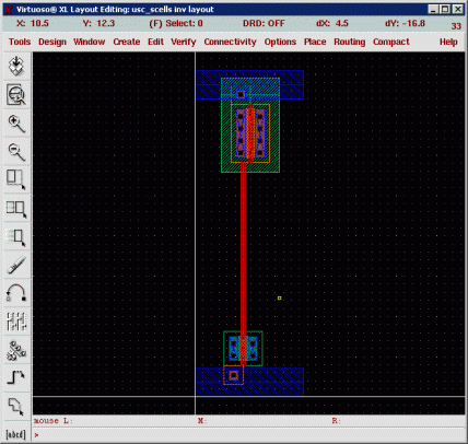
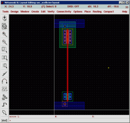
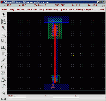
Oops. The PMOS, contact, and nwell need to be nudged to the left to make things match up. Select them all and move them to the left.
That's better. But wait, you say. Why are we using such a long poly wire to form the input to the inverter? Isn't poly a poor conductor? Won't the resistive load of this wire effectively slow down the gate?
Answer: Yes. Poly is a bad conductor. There are many reasons why it is done this way. First, contacts are even worse conductors. If we wanted a vertical metal1 wire for the inverter input, we'd need two contacts. One to bring the metal1 down to poly for each MOSFET channel. Instead, using a long poly wire means that we just need one contact to bring the input signal downto poly. Another reason is that it would be difficult to route the output wire if the input wire was in metal1 (especially for more complex cells).
Speaking of which, let's route the output. Select metal1 on your layer picker and draw a wire from PMOS source to NMOS drain.

Now draw the wires from the PMOS drain and NMOS source to the supply rails.
Now we need to form our input pin by addding a contact somewhere on the poly wire. To do this, we'll instance an "m1_poly" cell from the technology library (hit your O key). This is just a contact centered inside an overlapping poly square and metal1 square.
Normally, you could place this contact anywhere on the poly wire. However, things are a bit more complicated for us because we plan to use this cell with a place-and-route tool.
The basic idea is that we want all our input pins and output pins to be placed on a grid, where the grid size is selected such that wires may be easily routed on this grid and be guaranteed to be sufficiently spaced to not violate spacing rules. This is sometimes called a "routing track". Let's choose a grid size of 4.5 um, since this works with the height and width of the cell. It's common to offset the grid over your cell by half a grid space.
Therefore, the only legal values for the X and Y coordinate upon which our contact is centered are legal values of 4.5x+2.25, where x is an integer.
I'm going to place my contact at (2.25,24.75). Note you'll need to switch your layout editor snap grid back to half lambda (.15) to make this work. I'm also need to draw a short poly wire to connect the contact to the main poly wire.
The last thing we need to do is add the I/O and supply pins. First, we need to change a setting in the editor so Virtuoso will show the pin names. To do this, select Options | Display and turn on "Pin Names". Click "Save To", then OK.
To do this, select Create | Pin. You can specify the name for each, make sure you put the pins on metal1, and turn on "Display Pin Name". Also, make sure vdd! and gnd! are type "inputOutput", A is type "input", and Z is type "output". Each pin must be on the routing grid.
My Z output pin is at (11.25,11.25). The gnd! pin is at (2.25,2.25). The vdd! pin is at (2.25,38.25).
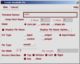
Place each pin in its appropriate location.

Now let's run a DRC to ensure that we didn't violate any design rules. If you have any, make sure you fix them now.

If you did have DRC errors, you can navigate the "markers" placed in the editor window by the DRC checker using the menu under Verify | Markers. This will allow you to find markers, zoom in on markers, and have the editor explain the purpose of each marker. I'll allow you to experiment with this when the need arises.
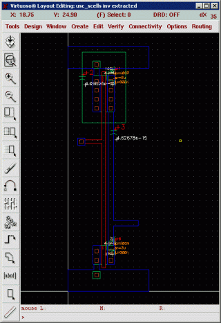
Now that we know we don't have any design rule violatations, save your layout with the topmost button on the layout editor. The next step is to extract our layout. Extraction simply means that the polygons that make up the layout are interpreted as a netlist, including devices (such as MOSFETs) and their associated connectivity. This is not quite as complicated as it sounds, since the MOSFET cells contain "active" layers that the extractor uses to easily identify MOSFETs and the source, drain, gate, and body terminals.
However, extraction does something else, too. It will recognize other implicit components in your design even if you didn't intend for them to be there. These components and their parameters are defined as a function of specific characteristics of your layout.
These are called parasitics, and are usually composed of capacitors formed from overlapping layers, and resistors that are are formed from wires. These parasitics only serve to hinder the performance of your design, but can only be recognized after you layout, since schematics don't contain any information about how your design is actually implemented.
The better the extractor, the closer your extracted design will match the reality of a fabricated circuit. Good extractors and good models together seek to provide simulation results that closely match the results you'd see if you tested the physical, fabricated version of your design.
The extractor is only as good as the extraction specification file that comes with your design kit. NCSU's extraction file is not capable of extracting parasitic resistance, only capacitance. But we have to live with this for now.
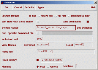
To extract, select Verify | Extract. Click "set switches" and select "Extract_parasitic_caps" and click OK. The other options can be left alone. Click OK. This will create a new view for your inverter called "extracted". Make sure you check your CIW window for extraction errors.
Go back to the Library Manager and open the extracted view for the inverter. This will show your layout annotated with parasitic capacitors (with their values). These parasitics are almost impossible to make out, but that's okay because we'll get a clearer picture of these parasitic values and locations when we generate a netlist for this layout. The other thing you'll notice in this view is that electrical connectivity is encapsulated. For example, if you click the Vdd rail, the editor will highlight all the layers that are electrically connected to Vdd.
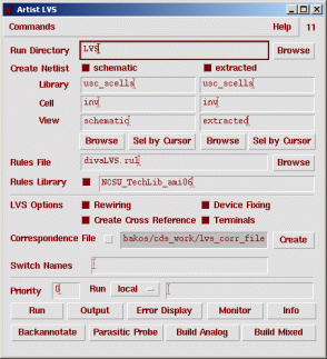
Now that we have an extracted design, we can perform another check to determine if our extracted layout schematic (netlist) matches the design in the schematic. This is called "layout-vs-schematic (LVS)". Select Verify | LVS. Make sure both the schematic view and extracted view are setup correctly, then turn on all the LVS options. Click Run.
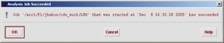
You should now see the following window. Click OK.
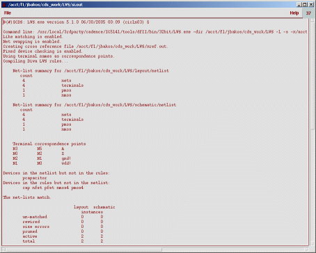
Now click the Output button on the LVS window. You will see an output log. The most important line here is the one that says, "The net-lists match.". If you see "The net-lists failed to match.", there's a problem with your layout. If this happens, carefully look over the log window and try to figure out the problem. Unfortunately, it is difficult to debug a layout based on the errors in this output log.
In order to simulate our extracted design, we need to build another type of extracted view. To do this, click "Build Analog" on the LVS window. Click OK on the new window.
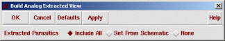
This creates another view for our inverter called "analog_extracted". This view is very similar to the extracted view, but is better suited for netlisting by Spectre.
Now we can simulate the extracted design. The simulation results of the extracted design should match the results from your schematic, except for performance degration due to the parsitics. Let's try it!
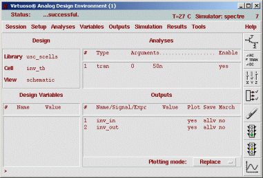
Go back to the Library Manager, open the inv_tb schematic, and select Tools | Analog Environment. Once Spectre comes up, load your previous state by selecting Session | Load State, and click OK.
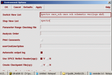
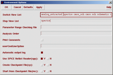
There's an additional setting we must make in order for Spectre to read the extracted netlist for the inverter instead of the schematic netlist. Select Setup | Environment. In the window, add "analog_extracted" to the beginning of the "switch view list". This will give presidence to analog_extracted views for netlisting.

Let's also delete our "current" outputs from the outlist, and just leave inv_in and inv_out.
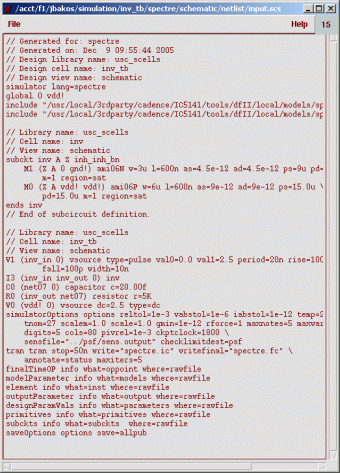
We should verify that Spectre has indeed read the analog_extracted version of the inverter. To do this, let's take a look at the netlist for the inverter. Select Simulation | Netlist | Create.
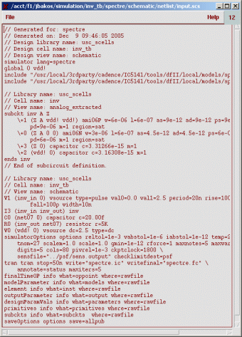
Verify that the inverter subcircuit has a comment that says it is the analog_extracted view. Now, notice that there are two capacitors in the inverter that weren't there in the schematic version. These are the parasitic capactors. The first is the parasitic capacitance between on output (Z) and second is supply capacitance. Notice that both of these capacitances are about 3 femtoferads.
Notice that the extractor did not output any MOSFET gate capacitances. Why is this? This is an EXTREMELY important consideration. The reason is that the MOSFET models themselves include this capacitance, so there's no reason for the extractor to add extra capacitance here. However, the extractor did not output any fringe capacitance that exists between near-by wires. This is really bad. Also, it did not output any series resistance from any of the wires. It did not output any series inductance in any of the wires. Although to date NO extractor is able to extract inductance. An accurate algorithm for extracting inductance is an open research problem in CAD/design automation. Nevertheless, all wires do indeed have series inductance and this does inductance affect performance of fabricated chips.
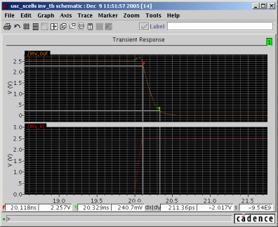
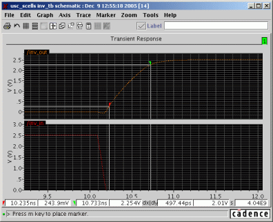
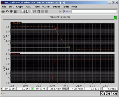
Let's simulate this circuit and determine the rise-fall times.
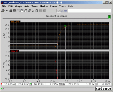
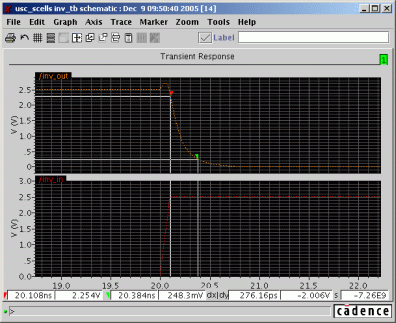
Rise time is 285.93 ps and fall time is 276.16 ps. As an added bonus, notice that our inverter is better balanced than in our previous simulations.
Now, let's determine exactly how much effect that paracitics had on our circuit. In Spectre, go back to Setup | Environment and DELETE analog_extracted from the "switch view list".
Create another netlist and verify that we're now using the schematic version of the inverter.
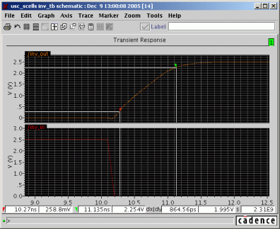
Now resimulate and measure rise/fall times.
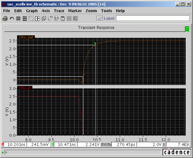
Rise time is 270.45 ps and fall time is 273.45 ps. The rise and fall times are slightly less. This shows that for this simple circuit, the parasitics didn't affect the performance much. However, this is mostly due to the fact that this is a small and simple circuit.
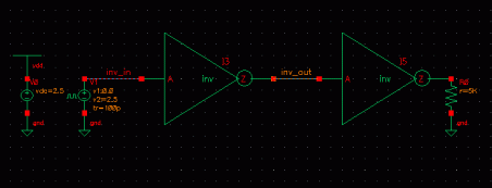
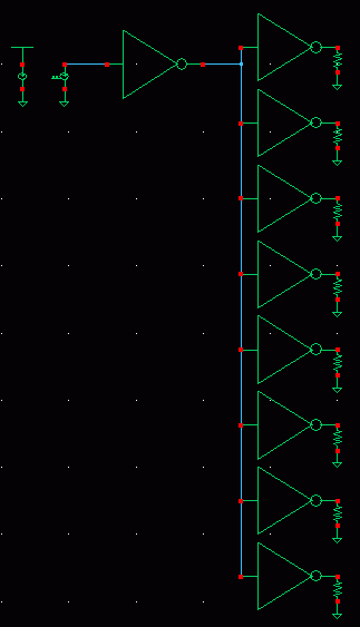
As the last exercise of this tutorial, let's change the testbench such that the inverter drives more a realistic load than the simple RC model that we previously used. First, go back to Setup | Environment and put analog_extracted back to the beginning of the "switch view list".
Next, open the inv_tb schematic. Let's remove the resistive and capacitive load and replace it with another inverter instance. Tie the output of the load inverter down with a 5K resistor to ground.
Simulate the new testbench and determine the rise/fall times.

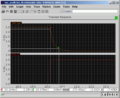
Rise time is 220.22 ps and fall time is 211.36 ps. Now let's try a fanout of 2...

Simulate the new testbench and determine the rise/fall times.
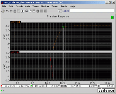
Rise time is 307.05 ps and fall time is 302.35 ps. Now let's try a fanout of 4...
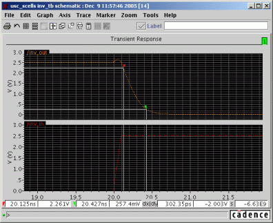
Simulate the new testbench and determine the rise/fall times.
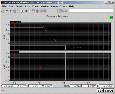
Rise time is 497.44 ps and fall time is 498.78 ps. Now let's try a fanout of 8...
Simulate the new testbench and determine the rise/fall times.
Rise time is 864.56 ps and fall time is 874.00 ps.
The following table summarizes these results.
| Fanout | Rise (ps) | Fall (ps) |
|---|---|---|
| 1 | 220.22 | 211.36 |
| 2 | 307.05 | 302.35 |
| 4 | 497.44 | 498.78 |
| 8 | 864.56 | 874.00 |
This table demonstrates the effect of loading a logic gate. Note that a popular logic delay metric, called FO-4, is a technology-dependent unit that defines the delay of a minimum-sized inverter loaded by 4 copies of itself. Therefore, the FO-4 delay of the AMI C5N process is approximately 500 ps.
Bear in mind that if we loaded our inverter with other, larger gates, the load would be increased.
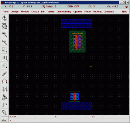
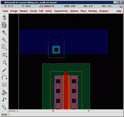
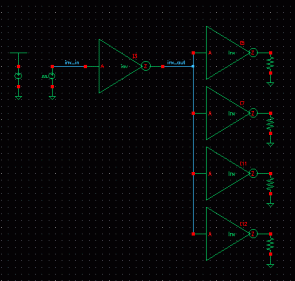
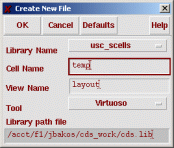
There's another thing that we need to consider for our layout. We want to be able to snap these cells together, both horizontally and vertically. We need to make sure that we can do this without violating any design rules. Let's create a new layout and see if we can snap together four inverters in two rows.
Create a new temporary layout view called "temp". Place four inverters in the following manner.
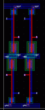
Notice that I flipped the inverters on the top row in order to match the Vdd rails.
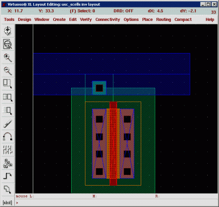
Even without running a DRC check, we can see that there are 2 problems here. First, the nwells of vertical PMOSs don't match up. Also, it would be nice to join the nwells of adjacent cells into a single contiguous region. We can fix both these problems by extending the nwell in the inerter cell such that it meets the edge of the rails (sides and top). We can do this by opening up our inverter layout and making the change there.

Do a DRC and save your layout.
Go back to your temporary layout and you'll see that it has been automatically updated to reflect the change in your inverter layout.
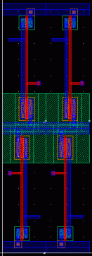
Now run a DRC check on this design to ensure that there's no metal1 spacing violations between adjacent cells. If so, we may need to increase the length of our supply rails.
If you don't have any DRC violations, then perform another extraction, LVS, and analog extraction.
That's all for this tutorial! Next we'll learn how to characterize a logic cell library with Cadence SignalStorm!