This tutorial will introduce you to VHDL Design using Mentor's HDL Advantage. In this tutorial, you will be guided through the design of an adder datapath cicruit.
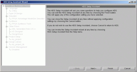
First, switch to your mentor work directory and type "fa_with_pp". The first thing you'll see is the "HDS Setup Assistant Wizard" window. Click Cancel.
After this, you'll see the HDL Designer Library Manager. This library manager serves the same basic purpose as the Cadence Library Manager. First, kill the "Launch Pad" frame by clicking the small arrow pointing to the right in the upper-right hand corner of the frame.
In HDL Designer, a "project" is simply a set of library mappings. Library mappings are used to associate each library name with a set of paths where designs are stored.
Right now you're looking at the example libraries that are mapped as part of the "example" project.
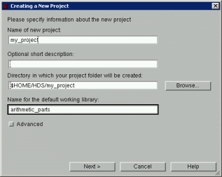
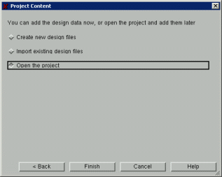
Let's create a new project. Select File | New | Project. Give the project any name you wish. Whenever you create a new project, HDL Designer forces you to create a new library as well. Let's name the library "arithmetic_parts". Click Next.
Click Next on the second window.
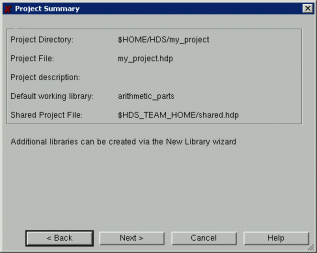
On the third window, select "Open the project" and click Finish.
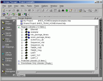
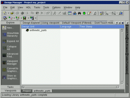
You will now be returned to the Design Manager. The Design Manager is currently displaying the designs (called "components" in HDL Designer) that are stored in the arithmetic_parts library.
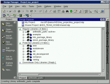
Switch over to the Project tab (near the bottom of the window). Here you'll see all the libraries that are currently mapped in your project. As you can see, there are three types of libraries: regular, protected, and downstream only. Regular libraries are intended for design entry, protected libraries are read-only and are intended for shared components and HDL packages, and downsteam-only libraries are indended for pre-compiled IP (as opposed to graphical or HDL designs).
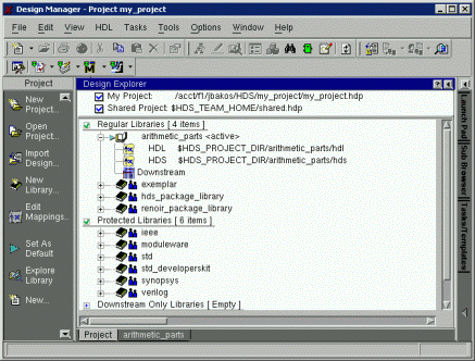
You can also see the library mappings if you expand one of these library names (using the plus sign to the left of the name). For example, if you expand the "arithmetic_parts" library, you'll see the library mappings for our new library. The "HDS" mappings show where graphical representations of your designs will be stored, and the "HDL" mappings show where the HDL representations of your designs will be stored.
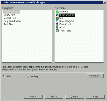
Let's begin adding designs to our library. First, let's design a 4-bit carry-lookahead adder. Select File | New | File. Select "Graphical View" in the left pane and "Block Diagram" in the right pane. Click Finish.
You will now see the block diagram editor.
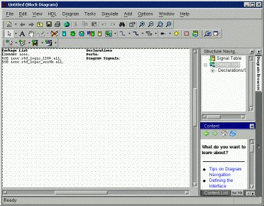
First, feel free to close the pane on the right.
The first thing we should do is add the I/O ports that make up the interface. For a 4-bit adder, the interface is comprised of the two 4-bit input values, a single-bit carryin value, a 4-bit result value, and a single-bit carryout value.
Click the down-arrow next to the toolbar button that looks like a thick wire. This is the "add bus button", which is used to add multiple-bit signals to a design. One of the sub-options is "add bus with a port".
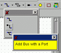
Click the "add bus with port" option and draw a short wire segment to the left side of the editor window. Just like in Cadence, you'll need to hit your escape key to exit out of the "add bus with port" mode.
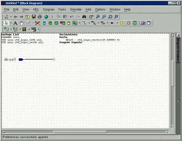
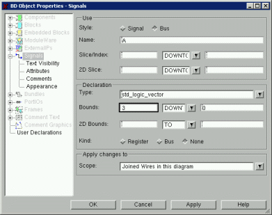
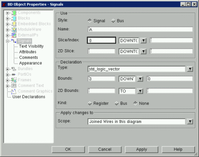
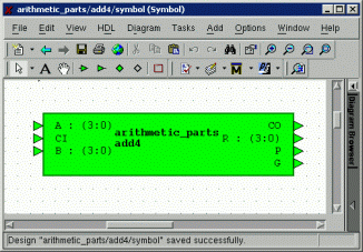
Any wire connected to a port becomes part of the interface for the design. The port takes on the characteristics of the wire or bus connected to it. You can't directly name a port. The port's name matches the name of the wire or bus that's connected to it. We just added a bus that is connected to an input port. The default name for the wire is "dbus0", the default type is std_logic_vector, and the default width is 16 bits. Let's change this. Double-click the wire to open the properties window. Change the name to A and the width to 4 bits. After you do this, click OK.
Add the B input port and bus the same way. The final input, carryin, is only a single bit, so you'll have to add this port using the "add signal with port" button (next to the "add bus with port") button. The corresponding type will be "std_logic", which is used for single-bit wires. Name this sigal "CI".
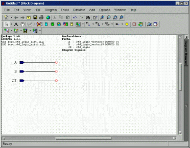
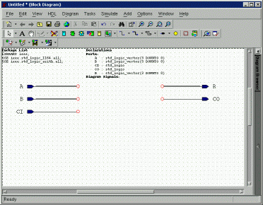
In order to add the output ports, we'll need to add the buses/wires and output ports independently. Change the bus and signal buttons such that you can add busses and signals without ports. In order to add an output port, you'll need to click the down-arrow next to the port button and change the mode to "output port". Add the output ports for "R" and "CO".
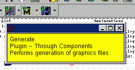
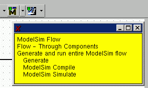
Now let's generate VHDL for our design. Click the "Generate Through Components" button.
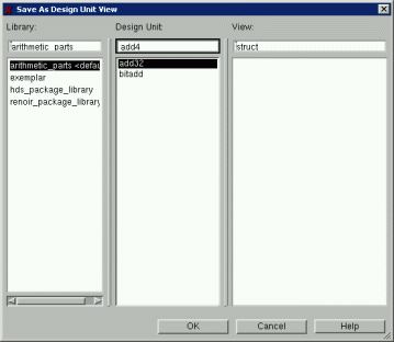
When you click this button, you'll be notified that you must save the design first. Name the component "add4".
Now let's view the generated VHDL. Select HDL | View Generated HDL. You'll get a read-only VHDL editor displaying the following VHDL.
		-- VHDL Entity arithmetic_parts.add4.symbol
		--
		-- Created:
		--          by - jbakos.faculty (hermes.cse.sc.edu)
		--          at - 22:38:55 12/22/05
		--
		-- Generated by Mentor Graphics' HDL Designer(TM) 2005.1b (Build 6)
		--
		LIBRARY ieee;
		USE ieee.std_logic_1164.all;
		USE ieee.std_logic_arith.all;

		ENTITY add4 IS
		   PORT(
		      A  : IN     std_logic_vector (3 DOWNTO 0);
		      B  : IN     std_logic_vector (3 DOWNTO 0);
		      CI : IN     std_logic;
		      CO : OUT    std_logic;
		      R  : OUT    std_logic_vector (3 DOWNTO 0)
		   );

		-- Declarations

		END add4 ;

		--
		-- VHDL Architecture arithmetic_parts.add4.struct
		--
		-- Created:
		--          by - jbakos.faculty (hermes.cse.sc.edu)
		--          at - 22:38:55 12/22/05
		--
		-- Generated by Mentor Graphics' HDL Designer(TM) 2005.1b (Build 6)
		--
		LIBRARY ieee;
		USE ieee.std_logic_1164.all;
		USE ieee.std_logic_arith.all;


		ARCHITECTURE struct OF add4 IS

		   -- Architecture declarations

		   -- Internal signal declarations


		BEGIN

		   -- Instance port mappings.

		END struct;
Let's take a closer look at this VHDL. First, you'll notice that we have an entity and architecture in this file. The entity simply defines the interface for the component and the architecture defines the behavior of the component. Currently, the architecture is empty, since we haven't defined any behavior yet.
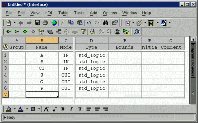
Let's begin to define our behavior. To do this, let's create a new component that will be used to accept single-bit inputs from A and B. This component will contain a full adder and generate/propagate logic. We can implement this component as a truth table.
Select File | New | File from any of the HDL Designer windows. Select "graphical view" in the left pane and "interface" in the right pane. Use the interface editor to setup the I/O as shown.
Now that we have the interface setup, let's check out the symbol that was automatically generated. Expand the right pane and click "Symbol".
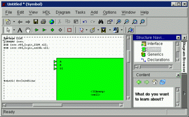
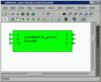
You'll notice that the symbol doesn't look very good. First, save the symbol and name it "bitadd". Now, edit the symbol to make it smaller. You will probably need to use the zoom button on the toolbar.
Once you're done, double-click the symbol. In the window that pops up, click "VHDL File" in the left pane and "Combined" in the right pane. Click Next. In the next window, type "bitadd" as the architecture name. Click Finish.
You will now see the VHDL editor. In the architecture, between the BEGIN and END, add two simple concurrent assignment statements:
S <= A xor B xor CI;
G <= A and B;
P <= A or B;
Save the file and close the editor.
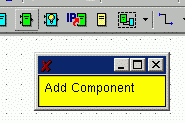
Now return to the block diagram editor for the add4 component. In order to create an instance of another component, you need to use the "Add Component" button.
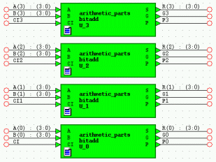
In the window that appears, drag the bitadd component into the block diagram. Next, do a right-click on the component and select "Add Signal Stubs" on the pop-up menu. Click OK in the next two windows that appear. Adjust the properties of the input/output signals such that the A and B inputs consist of bit 0 of the corresponding busses...
...and the S output consists of bit 0 of the R bus and add a "0" suffix to the P and G signals. Leave the CI input named CI, as it will be implicitly connected to the CI signal as the top-level input.
Now add three more bitadd components, adding signal stubs, and renaming the input and output ports as appropriate.
In order to add the carry-in logic, we can use embedded blocks. Embedded blocks provide a way to add short blocks of VHDL directly into the block diagram VHDL file. Click the embedded block button...
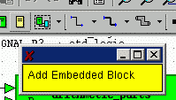
Place an embedded block in the diagram.
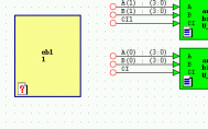
Once you do this, double-click the embedded block. A window will appear asking what view you'd like to add. Make sure "text" is selected and click OK.
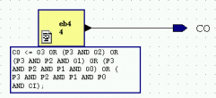
Type in the carry-in logic for bit 1, which is CI1 <= G0 OR (P0 AND CI);. After you do this, resize the text window and the embedded block. Move the embedded block such that you can connect it to the CI input of the full adder for bit 1.
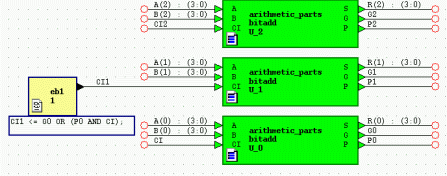
Repeat this operation to add the carry-in logic for the other full adders.
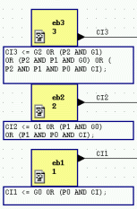
Now let's add the carry-out logic.
If you'd like, you can clean up the diagram to make it look a little cleaner.
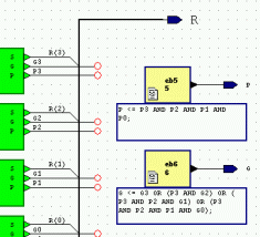
If we want to use our 4-bit carry-lookahead adder as part of a larger adder design, we should add a supergenerate and superpropagate output. This way, when constucting a larger adder from these adders, we can achieve a constant total latency for computing the carryins for each 4-bit adder.
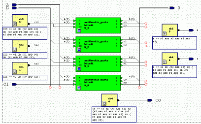
Add embedded blocks and additional output ports for the supergenerate and superpropagate.
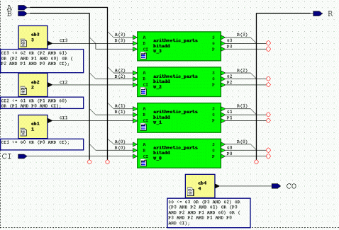
Here's another look at the completed block diagram.
When you save the diagram, the new outputs will be added to the symbol automatically. Use the Design Manager to clean up the symbol for the 4-bit adder.
Now let's generate and inspect the VHDL for our adder.
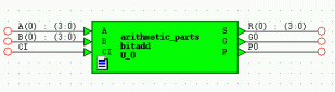
		-- VHDL Entity arithmetic_parts.add4.symbol
		--
		-- Created:
		--          by - jbakos.faculty (hermes.cse.sc.edu)
		--          at - 22:32:01 12/23/05
		--
		-- Generated by Mentor Graphics' HDL Designer(TM) 2005.1b (Build 6)
		--
		LIBRARY ieee;
		USE ieee.std_logic_1164.all;
		USE ieee.std_logic_arith.all;

		ENTITY add4 IS
		   PORT(
		      A  : IN     std_logic_vector (3 DOWNTO 0);
		      B  : IN     std_logic_vector (3 DOWNTO 0);
		      CI : IN     std_logic;
		      CO : OUT    std_logic;
		      G  : OUT    std_logic;
		      P  : OUT    std_logic;
		      R  : OUT    std_logic_vector (3 DOWNTO 0)
		   );

		-- Declarations

		END add4 ;

		--
		-- VHDL Architecture arithmetic_parts.add4.struct
		--
		-- Created:
		--          by - jbakos.faculty (hermes.cse.sc.edu)
		--          at - 22:32:01 12/23/05
		--
		-- Generated by Mentor Graphics' HDL Designer(TM) 2005.1b (Build 6)
		--
		LIBRARY ieee;
		USE ieee.std_logic_1164.all;
		USE ieee.std_logic_arith.all;

		-- pragma synthesis_off
		LIBRARY arithmetic_parts;
		-- pragma synthesis_on

		ARCHITECTURE struct OF add4 IS

		   -- Architecture declarations

		   -- Internal signal declarations
		   SIGNAL CI1 : std_logic;
		   SIGNAL CI2 : std_logic;
		   SIGNAL CI3 : std_logic;
		   SIGNAL G0  : std_logic;
		   SIGNAL G1  : std_logic;
		   SIGNAL G2  : std_logic;
		   SIGNAL G3  : std_logic;
		   SIGNAL P0  : std_logic;
		   SIGNAL P1  : std_logic;
		   SIGNAL P2  : std_logic;
		   SIGNAL P3  : std_logic;


		   -- Component Declarations
		   COMPONENT bitadd
		   PORT (
		      A  : IN     std_logic ;
		      B  : IN     std_logic ;
		      CI : IN     std_logic ;
		      G  : OUT    std_logic ;
		      P  : OUT    std_logic ;
		      S  : OUT    std_logic
		   );
		   END COMPONENT;

		   -- Optional embedded configurations
		   -- pragma synthesis_off
		   FOR ALL : bitadd USE ENTITY arithmetic_parts.bitadd;
		   -- pragma synthesis_on


		BEGIN
		   -- Architecture concurrent statements
		   -- HDL Embedded Text Block 1 eb1
		   CI1 <= G0 OR (P0 AND CI);

		   -- HDL Embedded Text Block 2 eb2
		   CI2 <= G1 OR (P1 AND G0) OR (P1 AND P0 AND CI);

		   -- HDL Embedded Text Block 3 eb3
		   CI3 <= G2 OR (P2 AND G1) OR (P2 AND P1 AND G0) OR (P2 AND P1 AND P0 AND CI);

		   -- HDL Embedded Text Block 4 eb4
		   CO <= G3 OR (P3 AND G2) OR (P3 AND P2 AND G1) OR (P3 AND P2 AND P1 AND G0)
		   		 OR (P3 AND P2 AND P1 AND P0 AND CI);

		   -- HDL Embedded Text Block 5 eb5
		   P <= P3 AND P2 AND P1 AND P0;

		   -- HDL Embedded Text Block 6 eb6
		   G <= G3 OR (P3 AND G2) OR (P3 AND P2 AND G1) OR (P3 AND P2 AND P1 AND G0);


		   -- Instance port mappings.
		   U_0 : bitadd
		      PORT MAP (
		         A  => A(0),
		         B  => B(0),
		         CI => CI,
		         G  => G0,
		         P  => P0,
		         S  => R(0)
		      );
		   U_1 : bitadd
		      PORT MAP (
		         A  => A(1),
		         B  => B(1),
		         CI => CI1,
		         G  => G1,
		         P  => P1,
		         S  => R(1)
		      );
		   U_2 : bitadd
		      PORT MAP (
		         A  => A(2),
		         B  => B(2),
		         CI => CI2,
		         G  => G2,
		         P  => P2,
		         S  => R(2)
		      );
		   U_3 : bitadd
		      PORT MAP (
		         A  => A(3),
		         B  => B(3),
		         CI => CI3,
		         G  => G3,
		         P  => P3,
		         S  => R(3)
		      );

		END struct;
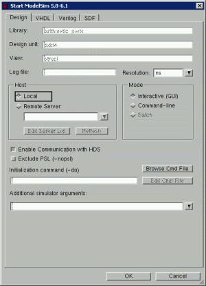
Now let's simulate our design. Click the ModelSim flow button.
Assuming you have no errors, you'll see the ModelSim startup window. Click OK.
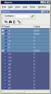
In the ModelSim window, you'll see four panes. The top-left pane shows the "structure". This reveals the hierarchy of your design. Selecting an instantiated component in this pane changes the context of the signals displayed in the signal (object) pane located in the top-center. The bottom pane is the command interface window. In the command interface window, type "view wave". This will open the wave window in the empty pane, located in the top-right. Undock the signal and wave panes by clicking the middle button in the top-right corner.

In the signal window, select the adder's interface signals, which are A, B, CI, R, CO, G, and P.
Drag these signals over to the wave window. Note: you can also right-click signals to add them to the wave window. You can also type "add wave [signal name]" in the command interface window. This is useful for scripting purposes.
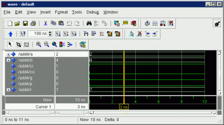
With the signals highlighted, do a right-click and select Radix | Hexadecimal. Now let's set the input
signals. In the command interface window, type the following.
force A X"2"
force B X"4"
force CI 1
run 10
Re-size and zoom into the wave window. You'll see that the result bus is 7, which is equal to 2+4+1. Carry-out, generate, and propagate are all 0, which is correct.
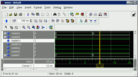
Now, type the following.
force A X"A"
run 10
You should see the following result. This time, the result is 10 + 4 + 1 = 15.
Now, type the following.
force A X"B"
run 10
You'll see the following results.
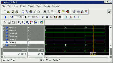
This time, the result is 11 + 4 + 1 = 0 with carry-out of 1. The propagate output is also 1, indicating that the carry-out is a result of a propagated carry-in. The generate output is 0, indicating that the two inputs themselves didn't generate a carry-out (it was propagated).
Also, you'll notice that the output transitions occur after zero time after the input transitions (outputs change simultaneously with the inputs). In other words, this circuit has zero latency. This is due to the fact that we don't have any technology information included with the circuit model. This simulation serves as a behavioral (functional) test only.
Try a few additional tests to ensure that your design is functioning properly. You can restart Modelsim by issuing a "restart -f" command. Script files (which, by convention, have a file extention of "DO") can be written in a text editor and executed by the simulator by typing "do [script path]".
When you're finished testing, close ModelSim.
Let's make things more interesting by using our 4-bit adder to build a 32-bit adder circuit. Create a new component as a block diagram view named "add32". My design is shown below.
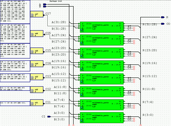
In case you can't read the VHDL from the screenshot, here's the VHDL for the carry-in embedded blocks.
Carry-in logic for 4-bit adders:
		   CI1 <= G0 OR (P0 AND CI);

		   -- HDL Embedded Text Block 2 eb2
		   CI2 <= G1 OR (P1 AND G0) OR (P1 AND P0 AND CI);

		   -- HDL Embedded Text Block 3 eb3
		   CI3 <= G2 OR (P2 AND G1) OR (P2 AND P1 AND G0)
		   OR (P2 AND P1 AND P0 AND CI);

		   -- HDL Embedded Text Block 4 eb4
		   CI4 <= G3 OR (P3 AND G2) OR (P3 AND P2 AND G1)
		   OR (P3 AND P2 AND P1 AND G0)
		   OR (P3 AND P2 AND P1 AND P0 AND CI);

		   -- HDL Embedded Text Block 5 eb5
		   CI5 <= G4 OR (P4 AND G3) OR (P4 AND P3 AND G2)
		   OR (P4 AND P3 AND P2 AND G1)
		   OR (P4 AND P3 AND P2 AND P1 AND G0)
		   OR (P4 AND P3 AND P2 AND P1 AND P0 AND CI);

		   -- HDL Embedded Text Block 6 eb6
		   CI6 <= G5 OR (P5 AND G4) OR (P5 AND P4 AND G3)
		   OR (P5 AND P4 AND P3 AND G2)
		   OR (P5 AND P4 AND P3 AND P2 AND G1)
		   OR (P5 AND P4 AND P3 AND P2 AND P1 AND G0)
		   OR (P5 AND P4 AND P3 AND P2 AND P1 AND P0 AND CI);

		   -- HDL Embedded Text Block 7 eb7
		   CI7 <= G6 OR (P6 AND G5) OR (P6 AND P5 AND G4)
		   OR (P6 AND P5 AND P4 AND G3)
		   OR (P6 AND P5 AND P4 AND P3 AND G2)
		   OR (P6 AND P5 AND P4 AND P3 AND P2 AND G1)
		   OR (P6 AND P5 AND P4 AND P3 AND P2 AND P1 AND G0)
		   OR (P6 AND P5 AND P4 AND P3 AND P2 AND P1 AND P0 AND CI);
Once you complete your design, inspect the generated VHDL, perform a functional test using Modelsim, and clean up its automatically generated symbol.
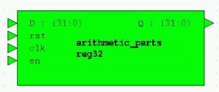
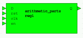
Now let's design a rising-edge sensitive 32-bit register and a 1-bit register. This will allow us to design a full pipeline stage, using our 32-bit adder in the datapath.
We need to be careful here. Recall that the DFF in my sample standard cell library did not contain a D-flip-flop with an asynchonous reset. Because of this, I need to make sure that my HDL does not require the use of such a flip-flop, otherwise this would cause a synthesis error. Therefore, the HDL design of my registers will assume a synchronous reset.
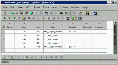
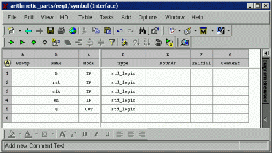
Create new components named "reg32" and "reg1" (use these names as the entity and architecture) as a Combined VHDL view. Create the interfaces (symbols) as shown.
reg32:
reg1:
Use the following VHDL code for the architecturess:
reg32:
		  clkd : process(D, CLK, EN, RST)
		    begin
		      if (clk'event and clk='1') then
		        if (rst='1') then
		          q <= "00000000000000000000000000000000";
		        elsif (en='1') then
		          q <= d;
		        end if;
		      end if;
		    end process clkd;
reg1:
		  clkd : process(D, CLK, EN, RST)
		  begin
		    if (clk'event and clk='1') then
		      if (rst='1') then
		        q <= '0';
		      elsif (en='1') then
		        q <= d;
		      end if;
		    end if;
		  end process clkd;
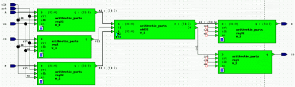
Now create another new block diagram component named "adder_datapath". Design it as follows.
Now let's simulate our design. Start up Modelsim. Undock the signals and wave window. Add the
interface signals (clk, rst, en, a, b, ci) and the internal signals (a1, b1, ci1, r1, co1) to the
wave window. Convert the radix to hexidecimal. To set up the clock signal, go to the signals window,
select clk, and select Edit | Clock and click OK. This will setup a clock signal with a 100 ns period
and 50 ns duty cycle. Check out the command interface window to see the Modelsim command that the
GUI generated to setup the clock. You can add this command to a script file for automated testing
purposes. Now type the following commands into the command interface window.
force rst 1
force en 1
run 150
force rst 0
force A X"00000004"
force B X"0000000A"
force CI 0
run 100
force A X"00000001"
force B X"00000002"
run 250
You should see the following output.
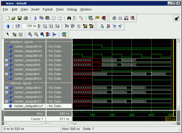
Notice how the inputs change the falling edge of the clock, while the outputs are changed on the rising edge of the clock.
We are now ready to proceed to the next stage of the design flow: synthesis!