In this tutorial, you will be guided through place-and-route of the 32-bit adder datapath using Cadence's First Encounter.
Switch to your encounter work directory and start up the tool by typing "encounter -simplefont".
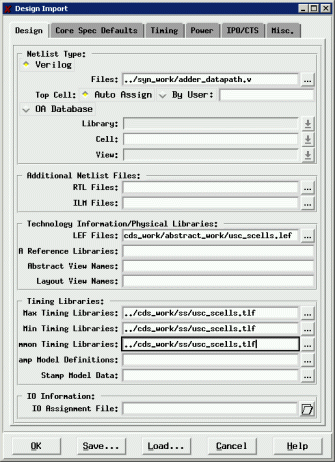
To start off, select Design | Design Import. Under "Files", browse-to and select the design netlist ("adder_datapath.v") from your synthesis work directory. This netlist specifies the schematic for the design. Also, select "Auto Assign" under "Top Cell".
Under "LEF Files", select the combined technology/abstract LEF file that you generated with Abstract Generator ("usc_scells.lef") from your abstract work directory. This file contains the fabrication information for the AMI C5N process (layers, design rules, layer per-square capacitance/resistance) as well as the abstracts (geometry, pin locations, internal route obstructs) for each of the cells.
Under "Timing Libraries", select the TLF file (usc_scells.tlf) from your SignalStorm work directory. Use this file for the max, min, and nomimal timing libraries. This file specifies the timing/delay information for each cell. This information is essentially the same as the information strored in the LIB/DB file. In fact, in this version of Encounter, you can actually specify LIB files here instead of TLF files. We generated the TLF file, so we might as well use it.
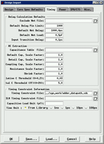
Go to the Timing tab. Under "Timing Constaint File" browse-to and select your timing constraint file (adder_datapath.sdc) from your synthesis work directory that you generated from Design Analyzer. This file only specifies the clock net and the clock period.
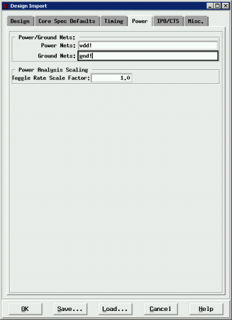
Go to the Power tab. Type in "vdd!" under Power Nets and "gnd!" under Ground Nets. These names are consistent with the supply net names we used from earlier in the design flow.
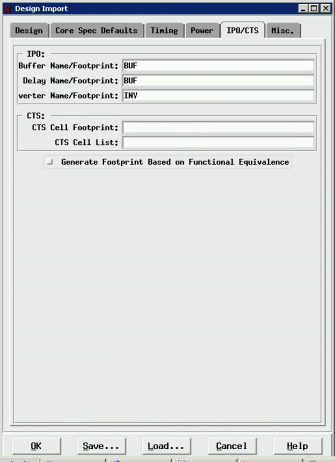
Go to the IPO/CTS tab. Type in "BUF" for the "Buffer" and "Delay" footprints and "INV" for the "Inverter" footprint.
If you'd like, you can save your import settings using the save button so you can load it later. Note: you may also want to save again after you specify your floorplan (later), since this information will also be saved.
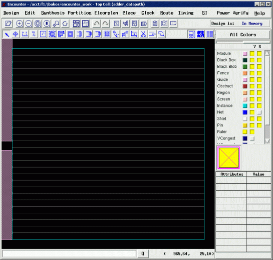
Now click OK. Check your terminal window to ensure that there were no problems during design import. Now is a good time to mention that you should check your terminal window everytime you do anything in Encounter (and sometimes you will need to scroll up). This is important because if error messages go unnoticed, you will think things are fine and not realize that one of your operations didn't complete successfully. Getting into this habit can be a big time saver!
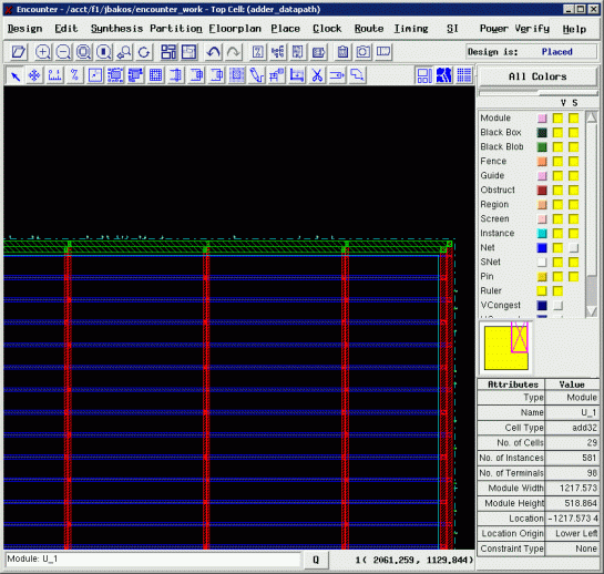
Your main Encounter window should look like the following.
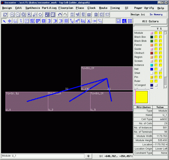
Also, notice that if you zoom out and scroll to the left, you'll see partitions for each of the top-level instances (as well as cell density relative to area utilization). In this screenshot, I clicked on the top module, which was the add32 module. Encounter shows us the this module is connected to the other three (registers).
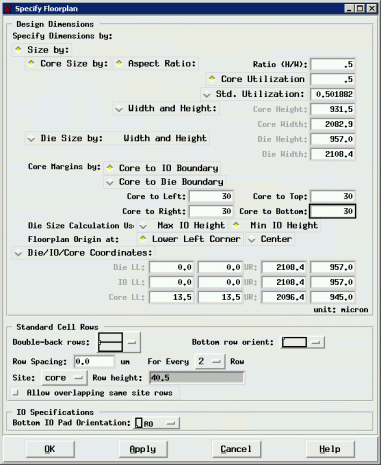
Select Floorplan | Specify Floorplan. Change the "Ratio (H/W)" to ".5", set the "Core Utilization" to ".5", and set the core margins such that there is a 30 micron margin on the top, left, right, and bottom.
The core utilization is the total core area divided by total cell area. It is used to compute the core area. We went with a conservative utilization to ensure that we have room to insert buffer cells. The margin is used for power rings. Click OK.
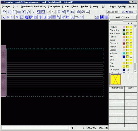
Your window will now look something like the following.
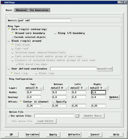
Now Select Floorplan | Custom Power Planning | Add Rings. Set the top and bottom layer to metal3. Set the widths to 9.9. Turn on "Center in Channel". Click OK.
Once you do this, hold down your right mouse button to draw a zoom box around the the upper-right corner of the power rings.
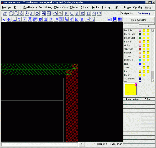
You can see the vdd and gnd rings that run around the core (horizontally in metal3 and vertically in metal2). You can also clearly see the vias that were generated to connect the corners of the rings.
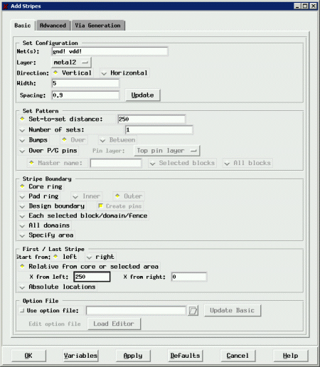
Now select Floorplan | Custom Power Planning | Add Stripes. Set the width to 5. Set the set-to-set distance to 250. Set the space from the left edge to 250. Click OK.
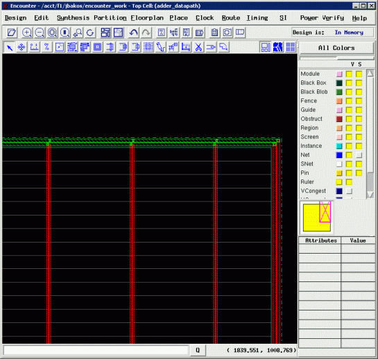
Now we have stripes that connect the power and ground rails with the rings (and helps with IR-drop). Again, observe the vias that were generated to connect the rings to the stripes.
Now we can route the power rails. Select Route | SRoute and click OK.
When you're zoomed in to the edge of the core (as I am in the above screenshot), you can see that the rails were even extended to catch the left-most vdd stripe. You can even select (left-click) a stripe or rail and check the properties on the right side of the window. This will show you the net to which the metal is connected.
You can see the vias that connect the vdd and gnd stripes to every other rail (alternating). You can also see the vias that connect the stripes to the rings.
Select Place | Place and click OK. This will place our cells. Fortunately, Encounter is careful to place the DFF cells in between the stripes since the DFF cells contain metal2 wires running horizontally throughout the entire cell. Placing a DFF cell underneath a stripe would cause a short between vdd/gnd and the internal wiring of the DFF cell. Of course, this is only possible if the stripes are spaced far enough apart to fit the large DFF cell in between the stripes.
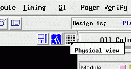
You won't see the placed abstracts until you put Encounter into "Physical View".
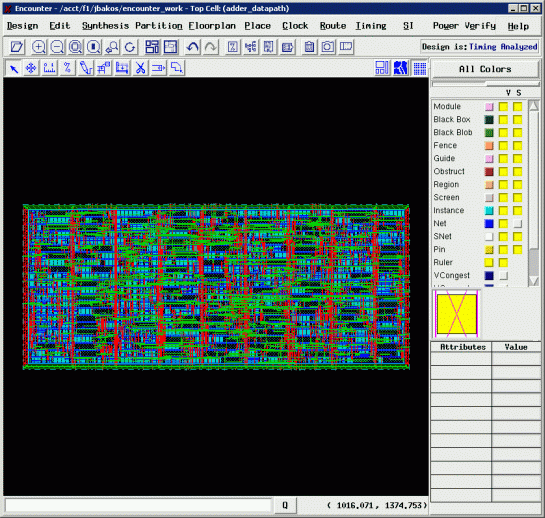
In the Physical view, your window should now look like the following.
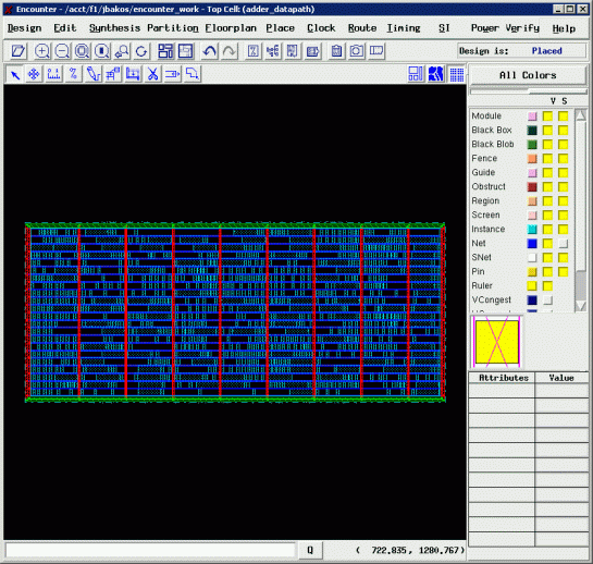
Zooming in will show the top-level I/O pins, as well as the internal I/O pins for each cell.
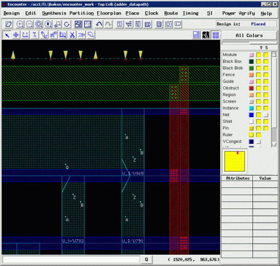
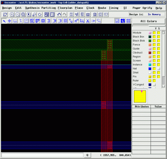
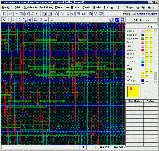
Here's a neat thing. Go back to the Floorplan view, scroll to the left, and click the add32 module (top-most). Now scroll back to the right and go back to Physical view.
You can now see which cells are part of the add32 module. It's interesting how they're distributed across the core area. This is due to the placement heuristic, which attempts to place connected cells closely together.
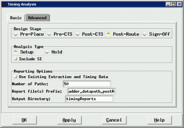
Now let's run a timing analysis. In timing analysis, Encounter will automatically perform a "trial route" (a low effort route), extract RC interconnect parasitics, and perform a timing analysis.
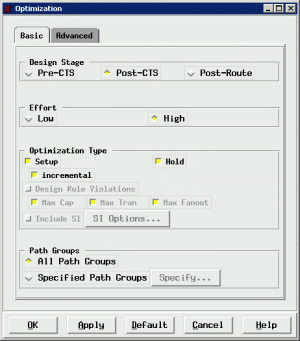
Select Timing | Timing Analysis. Under "Design Stage", notice that "Pre-CTS" is selected. This means that we're running timing analysis before clock tree synthesis. Click OK.
In the terminal window (from where you started Encounter), you will see if we have violated any slack.
I was told that my design has violated slack (timing requirement) by 11.738 ns. That's pretty bad compared to our entire clock period, which is 20 ns.
Recall that we met our timing requirement in Synopsys based on cell delays only. After adding interconnect parastics to the delay, we've consumed the previous slack and consumed over 70% additional time past the clock period!
This demonstrates that interconnect is a major delay factor in large circuits. The good news is that there are ways to improve these results.
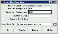
First, select Clock | Create Clock Tree Spec. Specify your buffer and inverter footprint name ("BUF", "INV") and click OK. This will generate a clock tree file.
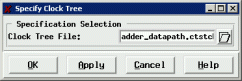
Select Clock | Specify Clock Tree. Click OK to have Encounter read in the clock tree file that we created in the previous step.
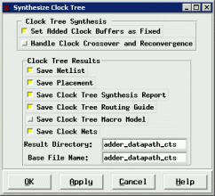
Select Clock | Synthesize Clock Tree and click OK. This step inserts clock buffers. It will take some time.
Now select Clock | Display | Display Clock Tree. Change the "Route Selection" to "Clock Route Only" and click OK.
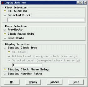
This will color the individual DFFs according to the phase delay.
Now select Clock | Display | Clear Clock Tree Display.
We can now perform timing optimization based on the clock tree we've inserted.
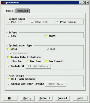
Select Timing | Optimization. In the window, select "Post-CTS" (Clock Tree Synthesis) and click OK.
After post-CTS timing optimization, Encounter reports that my setup slack violation is now 2.508 ns. A good improvement, but I'm still in violation of timing.
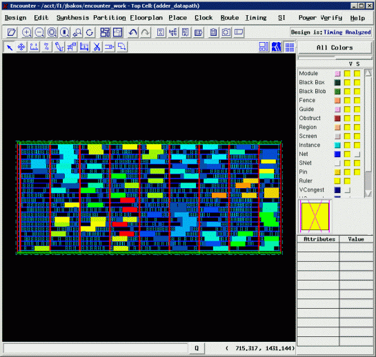
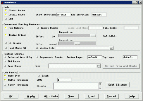
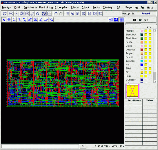
Now let's route the design. Select Route | Nanoroute. Turn on "Timing Driven" and turn the effort up to 10. Click OK.
We now have a routed design. Hit the F key to fit the design to the screen.
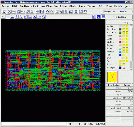
Notice that there's a design rule error near the top of the design. You may not get a design rule error. I find that I only see these errors in one out of every 20 or more nanoroute runs.
I believe that these errors may be caused by the overly conservative routing grid that we used for this design.
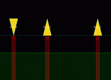
If you received such an error, you could either start over or fix the error yourself. If you would like to fix the error, first use your right mouse button to draw a zoom box around the error.
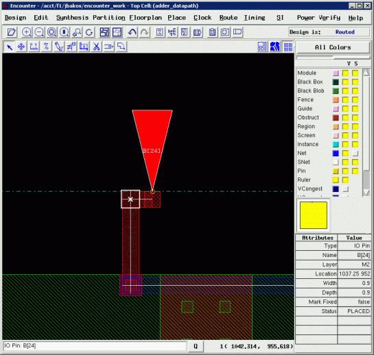
You can use the Move and Add Wire buttons to fix the error by moving the pin to the left and reconnecting its wire stub. Note: before adding wires, you need to hit your E key to enter the net name of the wire you want to add. Also, keep in mind that Encounter will only allow you to move pins on the 4.5 um snap grid.
Do not proceed until no design rule errors are indicated.
Now we can perform another timing optimization using the "Post Route" option. Select Timing | Optimization and select "Post-Route" and click OK.
According to the terminal window, my slack violation is now 3.097 ns. I am still in violation of timing, but I believe this may be due to my weak buffer design.
At this point, we need to insert filler cells to maintain nwall continuity.
Select Place | Filler | Add Filler. Enter "FILL" as the cell name and click OK.
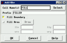
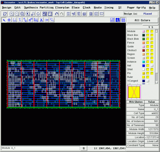
You'll notice that the entire core area is now filled in with cells.
Also, notice that the top-level I/O pins are located on the perifery of the "core" area.
Select Verify | Verify Geometry and click OK to perform a DRC check.
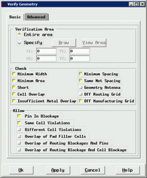
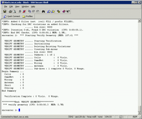
I didn't have any geometry violations. If you do, you can select Verify | Violation Browser to browse violations.
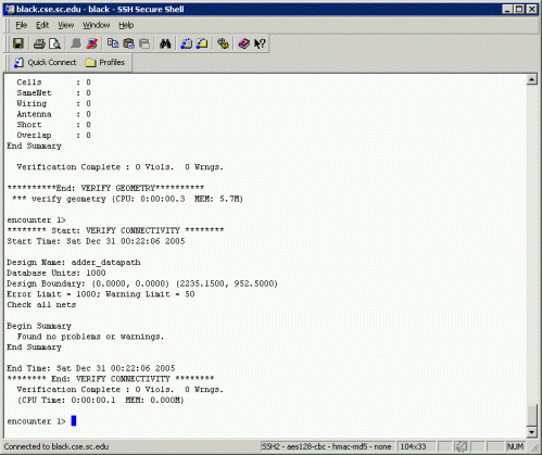
You can verify the connectivity of the design (missing routes, floating pins, etc.) by selecting Verify | Verify Connectivity and click OK. The results are shown in the terminal window.
At this point, Encounter can generate a final SDF file that includes both cell and interconnect delays. Select Timing | Extract RC and click OK, then select Timing | Calculate Delay and click OK.
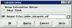
If you inspect the resulting SDF file, you'll see that we now have a complete SDF file, which includes both interconnect and cell delays. We can now bring in the Verilog netlist and this SDF file into Modelsim to achieve full timing verification.
However, our current netlist will not match the netlist from Synopsys, since Encounter has changed the netlist in order to add additional buffering. As such, in order to simulate this new design, you will need to save a new netlist. To do this, select Design | Save | Netlist and click OK. Use this new netlist to simulate your design. Assuming your placed-and-routed design is capable of running at the speed set in your DO file, you should be able to rerun the same DO file. If not, you may need to relax the timing information in this DO file (I had to bring my DO file down to 50 MHz).
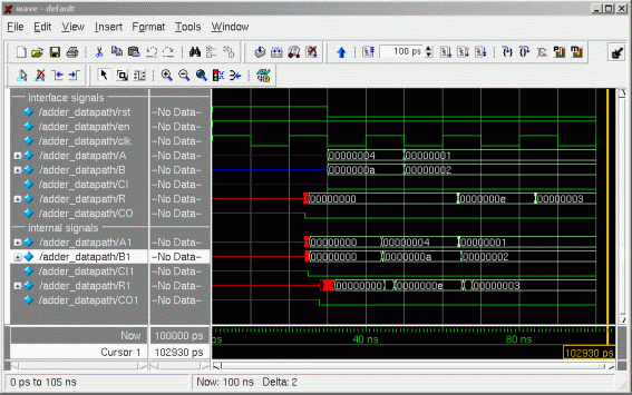
We can also use our simulation to determine the dynamic power consumption for our design for our test bench simulation. In order to do this, we'll need to perform a new Modelsim simulation using our new netlist and SDF model. However, this time, we'll tell Modelsim to dump a file that contains all the switching activity within our circuit during the test. This file is called a VCD (Value Change Dump) file.
In order to tell Modelsim to dump the internal switching activity, open your DO file and add the following lines to your script.
(after the restart line)
		vcd file adder_datapath.vcd
		vcd on adder_datapath.vcd
		vcd add -in -out -internal *
(as the last line)
vcd flush
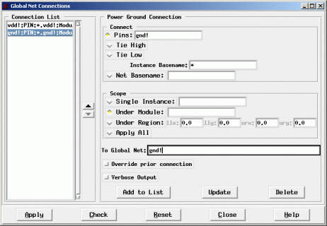
Back in Encounter, we first need to setup vdd and gnd as "global nets". To do this, select Floorplan | Global Net Connections. Under pins, enter "vdd!", under to global net, enter "vdd!", and click "Add to List". Repeat this procedure for "gnd!" and then click Apply then Close.
Now issue the following commands to the command-line interface.
setExtractRCMode -detail -noReduce
extractRC
updatePower -vcd ../syn_work/adder_datapath.vcd -vcdTop adder_datapath -noRailAnalysis -report power.rep vdd!
Note: the -vcdTop switch is useful when you're simulating a test bench design that includes a tester component and a component-under-test. In this situation, you'll use the vcdTop switch to tell Encounter to only analyze switching activity contained within the component-under-test.
Encounter will now tell you the dynamic and static power consumption for your circuit. My circuit consumed (on average) 1.0999 x 10^5 mw, or 10.999 nanowatts for the core logic leakage power, and 5.7728 milliwatts of switching power, as shown in the output.
		Delay calculation ...
		Topological Sorting (CPU = 0:00:00.0)
		Number of Loop : 0
		Start delay calculation ...
		delayCal using detail RC...
		Delay calculation completed.
		(0:00:00.1 85.000M 0)
		*** End delay calculation ***
		*** Delay calculation (cpu=0:00:00.1 mem=85.0M) ***
		INFO (SOCPARA-4303): Using voltage 2.5 V for all instances of
		net vdd!.
		For Net vdd! Instance Voltage Values:
		 1318 instances at 2.5 V
		Analyzing vcd vectors:

		*** Processing VCD file (cpu=0:00:00.0 mem=88.5M) ***
		power supply: 2.5 volt
		average power between 0.0000e+00 S and 1.0000e-07 S
		Total id in vcd file: 329
		    In module adder_datapath valid id: 329
		        redundant id: 0
		    In module adder_datapath invalid id: 0
		        redundant id: 0
		Total activity in vcd file: 1770
		    In module adder_datapath valid activity: 1770
		    In module adder_datapath invalid activity: 0
		average power(default) : 1.1257e+01 mw
		    average switching power(default): 5.7728e+00 mw
		    average internal power(default): 5.4846e+00 mw
		    average leakage power(default): 1.0999e-05 mw
		    user specified power(default): 0.0000e+00 mw
		average power by cell category:
		     core: 1.1257e+01 mw
		    block: 0.0000e+00 mw
		       io: 0.0000e+00 mw
		biggest toggled net: FE_OCPN171_B1_1_
		    no. of terminal: 3
		    total cap: 2.9211e+02 ff
		*** Power analysis (cpu=0:00:00.1 mem=85.0M) ***
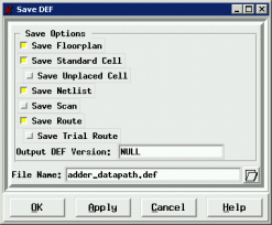
We also need to export a DEF (Design Exchange Format) file in order to read the layout into Virtuoso. DEF files are an easy-to-read text format.
Before you perform the export, make sure that you don't have anything selected in the Encounter window.
Select Design | Save | DEF and click OK.
Now would also be a good time to save your design in the native Encounter format. To do this, select File | Save Design. To load your design later, select File | Restore Design.
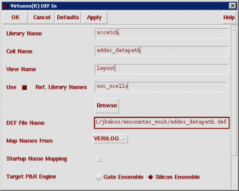
Back in the Cadence IC-Tools, you should create a new library to import your design. I called mine "scratch".
In the CIW, select File | Import | DEF. Fill in the target library, cell name, view name, reference library, and DEF filename. Click OK.
You will see a few hundred warnings here. These warnings are caused by a problem with the vias on the supply rings, stripes, and rails. This problem will prevent these vias from being imported into Virtuoso. To date, I have not found a solution to this problem. You may need to add these vias manually.
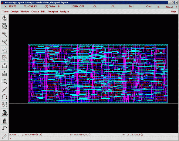
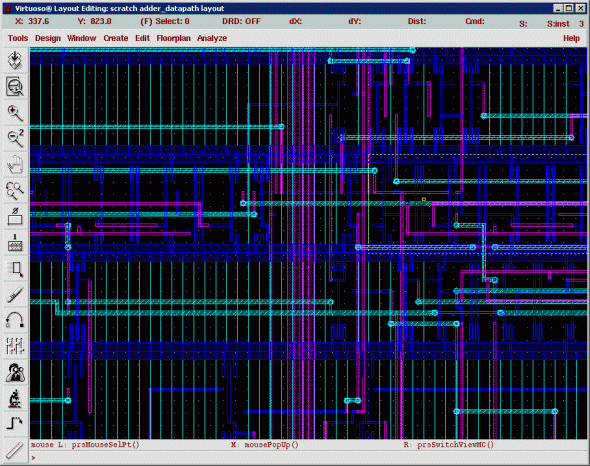
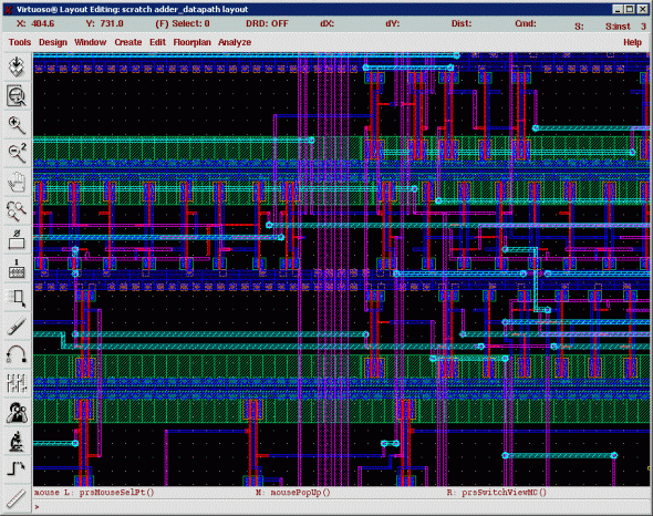
Open the imported design in Virtuoso.
Hit your E key to bring up the Display Options and set the view limit to 20 and click OK.
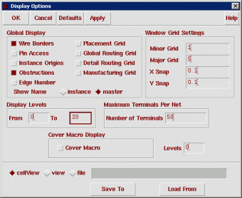
This will reveal the contents of the cells when you're zoomed in far enough. Each of the cells is instantiated as its abstract view.
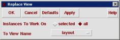
Select Floorplan | Replace View. Make sure the "To View Name" selection is set to "Layout". Select "Instances to Work on" to "all" and click OK. This will change all the cell views to layout.
After you do this, you'll view the generated layout as real layout. Notice the perfect nwell continuity!
You can now instance this cell in a larger, top-level chip design along with other top-level cells and I/O pads.
The only problem that remains is to manually add the appropriate vias to connect the supply ring, stripes, and rails (or figure out why the DEF Import isn't interpreting these properly from the DEF file).