As you have finished the design and test of the ALU unit, now is the time for your first CPU design.
This is a version of the R2000 CPU that is similar to the implementation
described in Chapter 5 of the Hennessy and Patterson text. You should be
intimately familiar with this design from your computer architecture class.
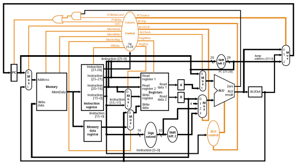
The block diagram below is reprinted from your text. In this unit, you will
implement everything you see in this diagram except for the memory unit
and you will test it by executing a MIPs program similar to the one
that you wrote for Lab 2.
In the multi-cycle CPU design, each instruction is executed in three to five
clock states, depending on instruction type. (refer to the handout for more
detailed information)
Note: Our next task will be to learn how to overlap these cycles in a pipelined design,
but for now each instruction will execute in three to five sequential states.

You have already designed the ALU and will find most of the other major
components that you will need in the CSELib library. This includes the
register file, the individual register components used for the instruction
register and the buffer registers. You will need to implement some
miscellaneous logic such as multiplexer, sign extension circuits, etc. The real
work for this assignment will be the control unit and its associate circuitry
shown in orange above: You will implement a finite state controller using the
FSM view in the mentor tools and using the discussion in chapter 5 of Hennessey
and Patterson as a guide.
To begin this task, define a new library called CPU, and create a new component symbol within that
library as shown below. You will have completed this unit when you have built
and simulated this component.

You may have noticed that the pinout of this component is almost the same as the memory component in
the digram above. This is because that diagram shows an entire MIPS based
computer system (needing only a clock input). In our case, you are implementing
a processor that accesses an external memory, hence the memory access pinouts
on your symbol.
Work on your CPU in small steps, testing parts of the design as you
implement it. For example, layout the components and test the datapaths
first, before you begin working on the control unit. Then, as you build
the control unit, implement and test each instruction type separately,
thoroughly test each new capability as you add them.
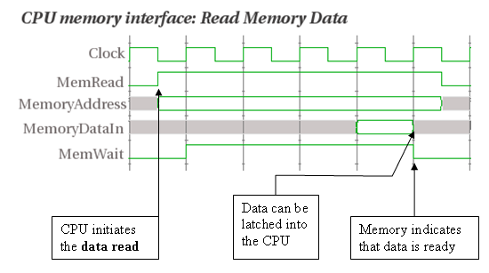
An example of a CPU executing a memory read:

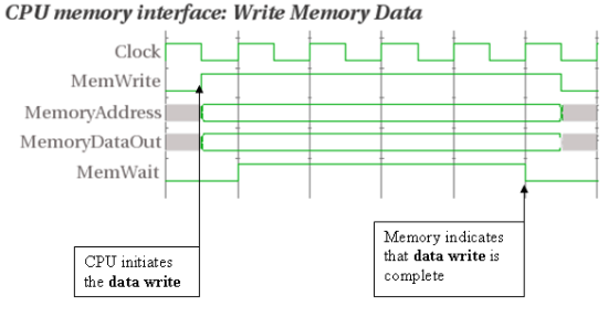
An example of a CPU executing a memory write:
