CSCE 211, Digital Logic
Design
Circuit
1
Due:
Thursday, October 7, 2010
Goal:
Generate 4 switched logic signals (A, B, C, D) and
display them with LEDs.
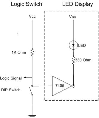
Each LED is said to be “buffer-driven” by a 74LS05 open-collector (OC)
inverter as shown
here.
Each gate in an OC device needs a resistive path to Vcc, which the LED
and resistor provide. The pin layout for the 74LS05 is the
same as for the 74LS04, which is part of the
74xx00
family.
A fifth LED circuit (with a “floating” input for now) will be used
later for displaying F(A,B,C,D). In effect, you are
creating a circuit that displays a row of a truth table. Your
circuits will be constructed on this
breadboard.
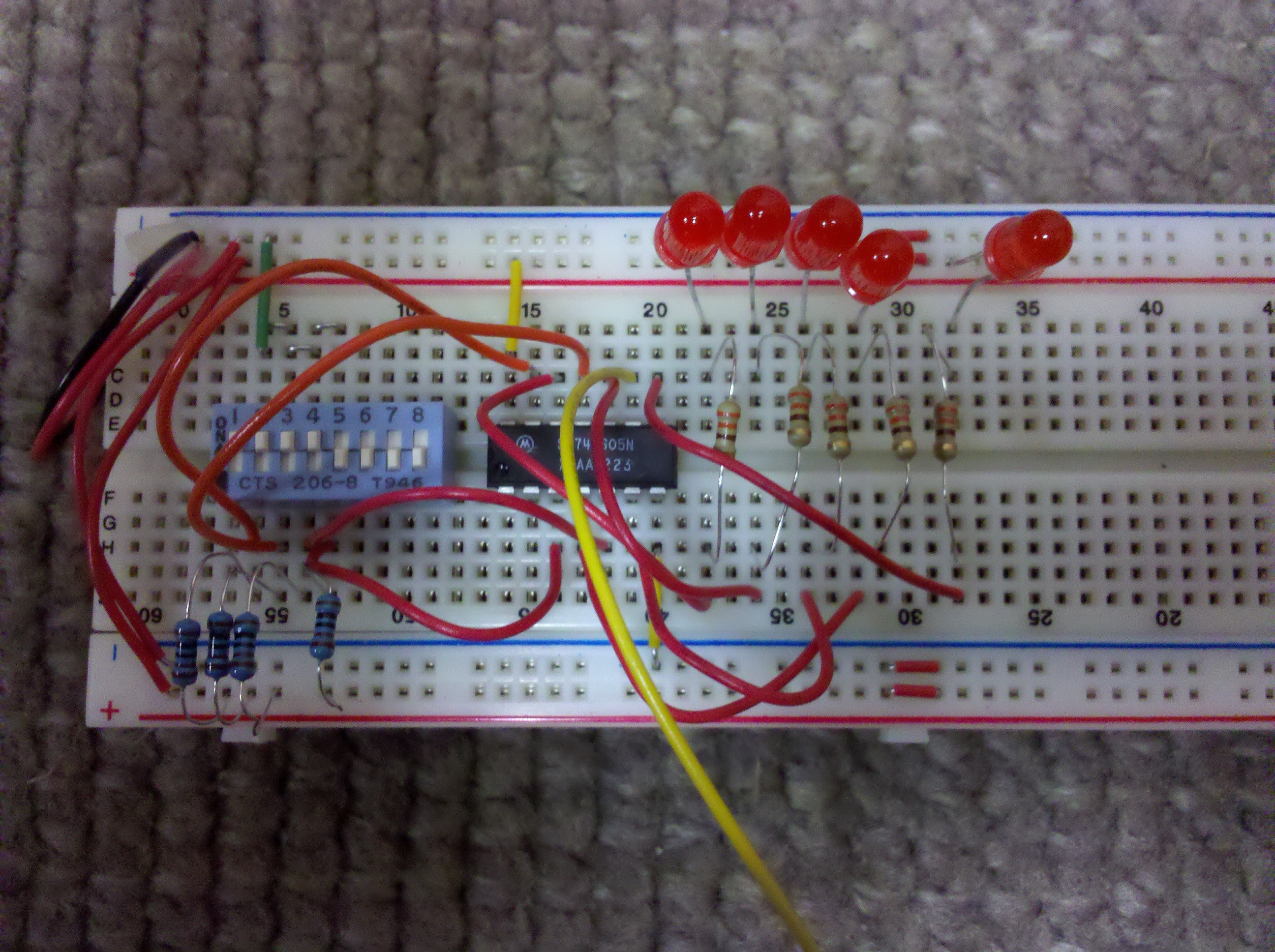
The details of constructing the first circuit will be explained in class
and are repeated on the next pages. A picture of finished Circuit 1 is shown here.
Materials needed:
1.
AA batteries (3)
2.
Breadboard with battery pack
3.
Blue 8-position, dual in-line-pin (DIP) switch
4.
Light Emitting Diodes (LEDs) (5)
5.
Resistors 330 ohm, Orange-Orange-Brown (5)
6.
Resistors 1.0 K ohm, Brown-Black-Red (4)
7.
Wire kit
The logic signals and displays
you build for this first project will be used in the next two experiments.
Try to make these circuits neat
and compact.
Grading: This
circuit project will be due on Thursday, October 7, in class and will be
worth 3 points toward your final grade. Your grade for each of the
circuit assignments will be based on (1) demonstrating that your
circuits work properly and (2) a short written report that
provides a few details about the circuits. You will
demonstrate your circuits and turn in your report in class on October 7.
Circuit
1 Report
- Draw a diagram of an LED
circuit with the DIP switch open. Explain why the
LED is ON.
- Draw a diagram of an LED
circuit with the DIP switch closed. Explain why
the LED is OFF.
- For each of the 4 signal
LEDs to the right of the 74LS05, identify the pin number of the inverter
output used. (For the “function value” LED to the right
of the other 4 LEDs, we have already selected pin #2 as the output.)
Circuit
1 Details
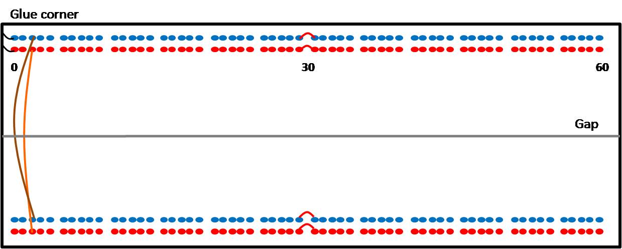
Power Busses
- Orient
the breadboard “horizontally” with the glued wires at the upper left corner.
-
Run a wire from the RED bus (Vcc)
at the top of the board to the RED bus at the bottom, and run a wire
from the BLUE bus (GND) at the top of the board to the BLUE
bus at the bottom. Place these two wires as close to the left side of the
board as possible to save space for future implementation.
-
On the top side, use one short wire (the short
red wire is appropriate) to connect the two RED holes that have the
number "30" between them, and use another short wire to connect the two
BLUE holes that have the number "30" between them. The purpose is to
bridge the gap in the RED bus and in the BLUE bus. Do the same
thing on the bottom side.
- Make
sure the wires are inserted tightly into the holes on the board.
LED
Test
- Above
and below the gap, there are columns of 5 electrically-connected
contacts. A wire inserted into one of these holes has the
same voltage (relative to GND) as the others.
- At
hole-location 32 insert the longer (+) leg of a red LED into the RED
bus.
-
Insert the shorter leg into location 32 below the bus.
- Bridge
a 330 ohm resistor (Orange-Orange-Brown) from the hole just below the short
leg of the LED to the other side of the gap at location 32.
- Connect
a wire from the “lower” side of the resistor to any BLUE
connection.
- Install
the two outer batteries into the battery pack. Do no
install the middle battery yet.
- Install
the middle battery and check that the LED is ON. If
not, check the polarity of the LED.
Inverter-LED
Test
- Pop
out the middle battery.
- Insert
a 74LS05 integrated circuit (IC), often referred to as a “chip,”
with pin 1 inserted into board location 14.
Make sure the “notch” of this IC, also called a “chip,” faces the
glued corner; pin 1 is then the pin in the lower left corner.
- To
provide power to the 74LS05 when batteries are installed, connect a wire
from pin 7 to BLUE. Connect another wire
from pin 14 to RED.
- Remove
the lower 330-ohm resistor wire, previously installed to BLUE, and
reconnect it to pin 2 of the 74LS05.
- Pop
in the middle battery and check that the LED is ON.
- Temporarily
connect a wire from pin 1 of the 74LS05 to BLUE. Confirm
that the LED turns OFF.
- Remove
the wire from pin 1 and let the inverter input “float-high.”
This lets us use the LED as an ON indicator for now.
Logic-Signal
Generation with DIP Switch and 1.0K Resistor
- Install
the blue DIP switch across the top gap with switch position 1 at
location 4. The left edge of the switch overhangs
so the left edge appears to be over location 3.
- At
the top of the switch “daisy chain” location 4 to 5, 5
to 6, and 6 to 7 with the short “U” shaped
wires.
- Run
a short wire from location 4 to BLUE.
- Install
another LED four holes to the left of the first LED; that is, insert into board
position 28. As noted below, this will be the LED
for the least significant variable, D.
- Use
a separate 330-ohm spanning resistor for this LED.
- Connect
a wire from an unused inverter output (for example pin 4) to the
lower end of D’s 330 ohm resistor. Test that D
is ON; confirm that the LED will go OFF when the inverter input (pin 3) is
grounded.
- Now
create a logic signal by connecting a 1.0 K (Brown-Black-Red)
resistor from the “bottom” of switch 4 to Vcc.
- Connect
a wire from the lower side of switch 4 to D’s inverter input (pin 3).
Test by using a retracted ball-point pen to move switch lever 4
up and down.
- The
LED will be OFF when the switch is in the up (“On”) position; the
LED will be ON when the switch is in moved downward. Read
“On” as NO to avoid confusion.
- Install
3 more LED circuits to the left of the D LED at locations 26, 24, and
22. They represent LED C, B, and A,
respectively.
- Install
a separate 330 ohm resistor for each LED and remember to use a separate
inverter input and separate 1.0 K resistor for each logic signal.
- Test
each LED circuit as you go along. Here is a piece of good
advice for you to follow: “Build a little;
test a little.”
- When
you finish, there will be 4 LEDs, each switched separately for the 4
variables.
- Make
sure that the switch positions and the LEDs correspond in going from left to
right.
Circuit
Hints
·
Design circuits, then build.
That is, first create the circuit’s logical diagram (supplemented by
pin numbers); then build.
·
Bends chip pins slightly to fit breadboard by
pressing gently pins against a firm surface.
·
Convention: place all IC notches towards the right-side
of the breadboard (towards battery pack).
·
Hot
chips spell trouble! Remove the middle battery and trouble
shoot.
·
Always use a 330 ohm resistor in series
with each LED. A “leg” or segment in a 7-segment display
is also an LED and requires a 330 ohm resistor.
·
Neat wiring is helpful.
·
Do not cross wires over chips so a chip
may be replaced easily if necessary.
·
Watch out for bare wires touching each other.
·
Tweezers or long-nose pliers are helpful in
inserting and removing wires.
·
To extract a chip from the board, use the
“finger” cap of a ball-point pen.
.