At this point you should have finished your multi-cycle CPU (including state controller) design. You have also simulated the design for correct execution of each instruction (one-at-a-time).
1) Reconcile the interfaces between memory operations on the CPU with
memory operation for the memory model. As you will see below,
there are significant differences between the control signals, bus
structure, word format,and timing of these two interfaces.
2) Model and simulate the entire system (memory and CPU) in the simulator.
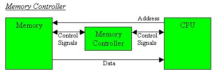
When you are done, this is a block diagram of what your design will look like.

Memory serves as a storage space for your data and program. The
Memory block shown in the above image is actually the MemoryModel component
in the CSELib library. The symbol for this component is show below:
You may have noticed that the signals at the pin-out of the MemoryModel and the
pin-out of your CPU do not match. In fact, they differ significantly
both in function and timing. The purpose of the MemoryController is
to rectify this difference. It will be a state machine that
accepts requests from the CPU for read or write operations, synchronizes
the CPU with the memory using the MEMWait signal, and manages the
interface to the memorymodel in order to make the transfer happen.
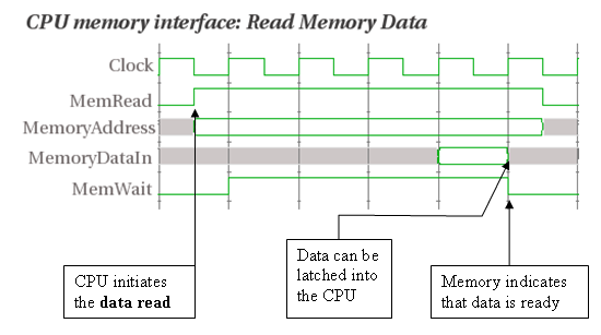
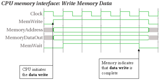
Memory operations from the CPU proceed as follows. Refer to the timing diagram below.
Clock cycle 1 -
the requested memory address is placed on the MemoryAddress out. Either
MemRead or MemWrite becomes active for a read or write operation
respectively.
Clock cycle 2 - the memory controller asserts MemWait back to the CPU
The CPU now holds in a wait state until the first clock edge (Cycle n)
after wait is de-asserted.
Clock cycle n -
The memory controller places read data on the data input bus and
deasserts MemWait. The CPU deasserts MemRead and latches the data into
the input buffer register at the end of this cycle to complete the read
operation.
(Note - a practical design choice would be to have
buffers on the input to and the output from the CPU, however if you
look at your CPU design you will see that these buffers are already in
place.)
To read data from the Memory Model, the first thing to do is to assert the MemBusReq_n
low. The "_n" indicates that this input is active low, so a '0' will activate. The
Memory Controller will then wait for the Memory Model to grant bus access via the MemBusGrant_n
signal. At that moment, the Memory Controller should see that it has access and
assert MemStrobe_n low, MemWriteSel_n high and the desired memory address to be read
on MemAddr_OutReg. The following cycle, we will release our bus request by raising
MemBusReq. If we wanted to initiate a burst read, we would continue to hold MemBustReq_n low
Once the Memory Model reads the data, it will output it on bus MemData_InReg.
The waveform is shown below:
The final block is this part of your design is the alignment logic. This
block has the function of reconciling the 32-bit word organization of
the memory withthe byte addresses coming out of the CPU. The first step
in this process is to realize that each memory word contains four byte
and thus the address input to the memory model will always be the CPU
address shifted right by two bits. The low order two bits will select
the particular byte lane within the 32-bit word that is returned.
We mentioned above that it is possible to point the memory model to an
initialization file through the generic declaraction attached to the
symbol. We will talk more about this in a moment. First, we need to know
how this file can be created. As an diagnostic program for your design
we have written as supplied to a test program written in MIPs assembler
called simpletest.s.
To familarize yourself with how this program works, you may wish to download a
copy and run it in the SPIM simulator. A full program listing with
load addresses and machine language shown is available in
simpletest.lst.
We have also prepared a loadable memory image of this program, with the
first instruction set up to load into memory location 0x000000. This
file can be found in simpletest.bin.
2) Modify the generic in your memory model component to point to this file.
3) Compile and run your design in the simulator. You should have setup
your reset line to force the PC to location zero. Start your simulation
run by toggling the reset line, then monitor the memory data bus as the
program executes. When finished you can monitor the data transfer of the
registers back into memory to verify your results.
Lets take a detailed look at each of these units.
Memory

The address size of the memory model is 24-bits. This address selects a
32-bit block of memory. When you add an instance of this componentto
your design, you will notice a "generic" declaration attached with a
pointer to a file. Using this generic, it is possible to initialize the
memory contents for the memory model from a text file in your work
directory. You will use this feature to load the memory with a
test program to be executed. See the section below on how to prepare
this program. Once prepared, modify the generic declaration that is
included in the symbol file to point to the file that contains your
program and recompile the design.
Memory Controller
To understand how this will work, lets begin with a description of
the memory interface signals coming to and from your CPU. These are the
signals shown to the right of the memory controller in the diagram
below. These read and write transfers are the same whether your CPU
is doing an instruction fetch, a load, or a store operation. (except for
differences in the read/write controls)

CPU to Memory Controller Interface


Memory Controller to MEMORYMODEL INTERFACE

Writing data to the Memory Model is similar to the read operation explained above. You should
be able to follow the waveform below and deduce its operation.

Alignment logic
The second part of the problem has to do with the fact when the CPU asks
for a byte or a word access, it always
expects that the byte will be in the low order 8-bits of the input bus.
However, unless the low order two bits of the address are zero, this
byte will not be in the low order byte lane of the memory word. The
function of the data alignment network is to examine the low order
two bits of the CPU address and in the case of LB instructions, shift
the selected byte lane of the incoming memory word to the low order byte.
An analogous problem arises for half-word accesses. Since there will be two
16-bit halfword lanes in each memory word.
Store byte and store half-word instructions present a special problem. If
the CPU asks to write a particular byte lane or half-word lane of a
32-bit memory work, you must do so without overwriting the other parts
of the memory word. Thus, Store byte and Store halfword instruction must
pre-read the contents of the memory word in question, insert the byte or
half-word and then write the memory word. Do this last, but you will
need to design both your control unit and aligment network to handle
this case.

Building and Running a Test Program
As mentioned in the class, there are two possible versions for the branch
implementation. If you implemented as stated in the textbook Appendix A
(NextPC = PC + Offset), then go ahead and use simpletest.bin. However,
if you implemented as stated in the diagramm in the middle of the book
and the branch description on the webpage (NextPC = PC + 4 + Offset),
then you should use the patched version of the bin file, which you can
get here:simpletest2.bin.
1) Make a copy of this file and place it in your group directory.